|
Altera MAX 7000S
Programming
Programming the EPM7128S
Using Quartus II
Quartus II is the
development tool for the full range of Altera
FPGAs and CPLDs, a free edition of the
software is
available to download from the
Quartus II Web Edition webpage. The
software is continually being updated as new Altera devices
are developed, at each software release, support for some
legacy devices may be dropped. At the time of writing this
page, the current version is Quartus II 13.1,
the last version to support the MAX7000 family was Quartus
II 13.0 SP1, legacy versions of the software are available
from the Quartus
II Web Edition downloads page.
As might be expected, Quartus II
is a very powerful and flexible tool, the downside of that
power and flexibility is the complexity of the software.
Altera have produced a large quantity of documentation and
training materials for Quartus II, a selection
of which are available for download from via the links at
the bottom of this page. This subset of the Altera document
suite and my notes on using Quartus II in
these pages only provides an introduction to the software,
covering the basics necessary to program the CPLD used in
MTXPlus+. For more comprehensive instructions, help and
training materials, refer to the
Quartus II Documentation page on the Altera website.
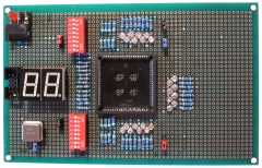
Hardware Test Bed
Rather than trying to go straight to
development of the glue logic for MTXPlus, I thought
that it was a better idea to experiment by developing
some test programs that could be executed on a simple
hardware test device.
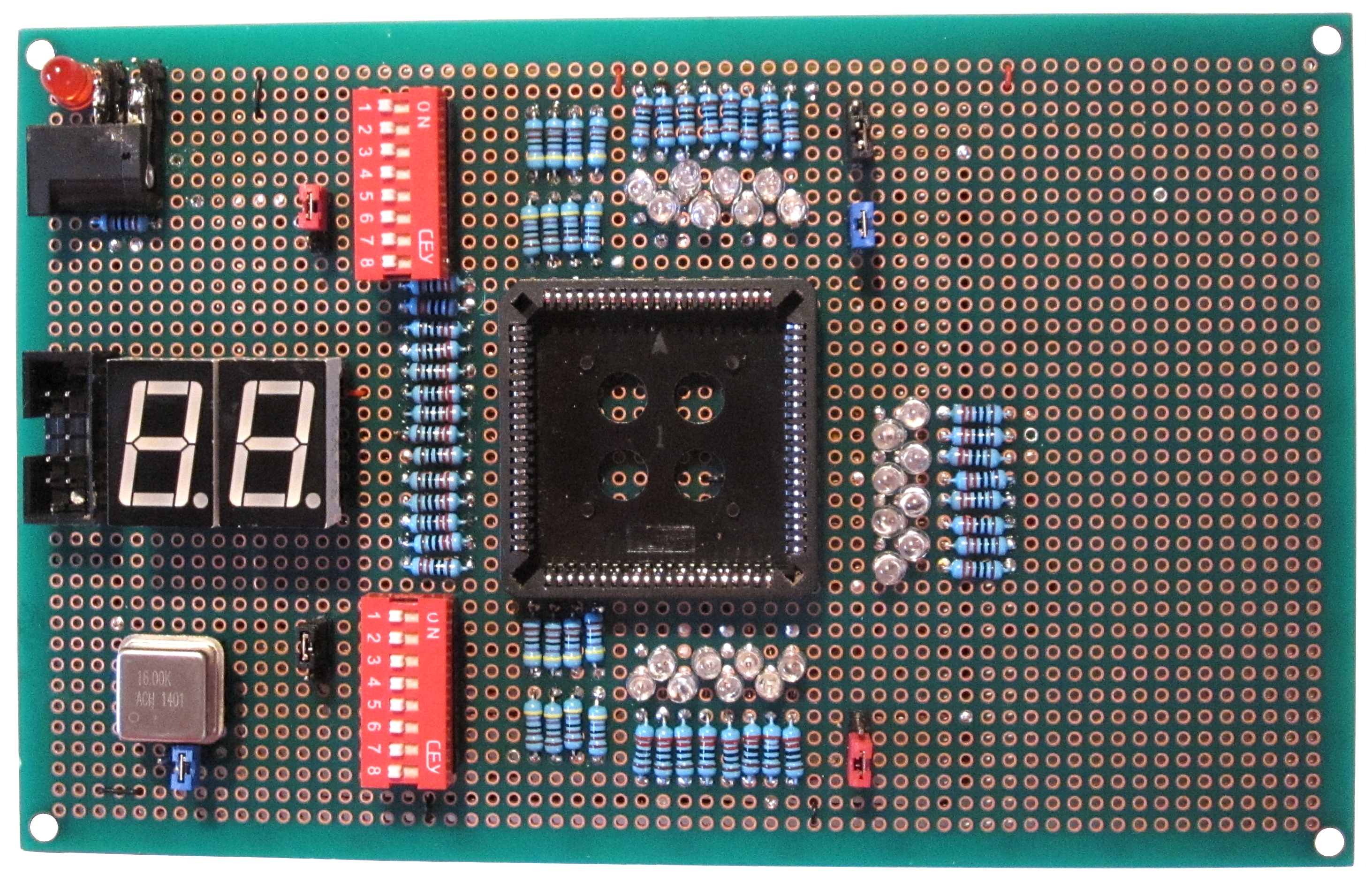
| To be able to exercise the programmed logic
and display the resultant outputs, a board with
basic inputs and outputs from switches and LEDs
will do the job, so I have built a hardware test
bed that was used to develop my skills and test
the MTXPlus CPLD logic.
You can find the
details on this page. |
 |
The test bed having done its job and given
me a little more confidence with Quartus II, I
was now ready to move on to developing the glue logic for
MTXPlus+. The remainder of this page gives a very high level
view of design development using Quartus II
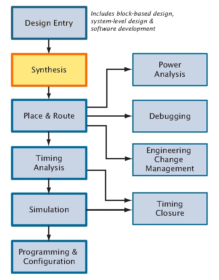
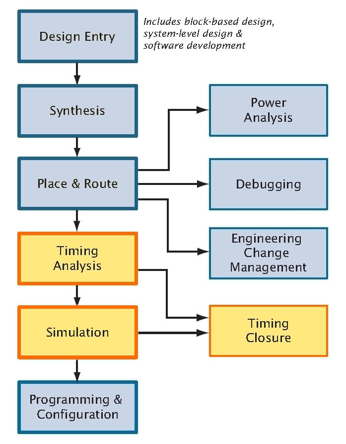
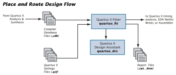
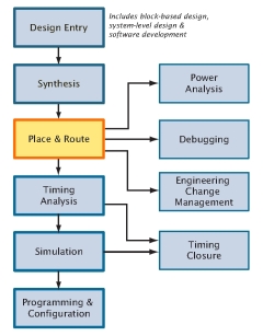
Quartus II Design Flow
|
Overview |
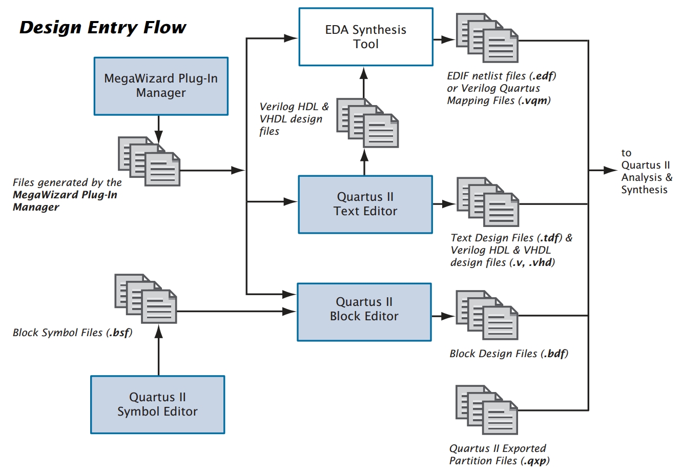
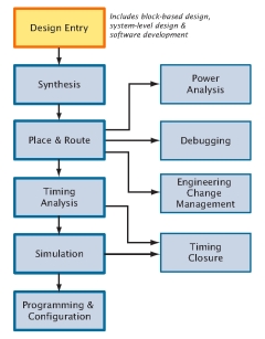
| Quartus II provides a fully
integrated suite of design components that are
available for use during all phases of CPLD and
FPGA design.
The flow chart opposite illustrates the
complete design process from creation of the
design through to programming of the target
device.
The various stages in the design flow are
well explained in the Quartus II
documentation. The Altera manuals should be the
primary reference when using the product. They
are comprehensive, that is very large, and many
of the topics are not relevant to small, CPLD,
designs such as mine. This page is intended to
give a minimal overview of Quartus II
and its use in MTXPlus+. |
 |
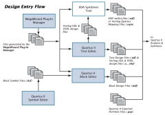
| Quartus II supports a number
of different design entry methods:
Schematic entry, block diagrams and
Hardware Description Languages (AHDL,
VHDL,
Verilog and
System Verilog). As the diagram shows, a
design can be developed using more than one type
of design entry method. To begin with, I shall
be using Schematic Entry - this should allow me
to get some familiarity with Quartus II
and the EPM7128S, including programming,
compilation, simulation, I/O allocation and
downloading to the CPLD through the JTAG
interface. I may need to use text entry at some
point to enter the memory decoding equations in
one of the
HDLs. |
 |
|
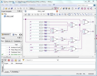
Schematic
Design Entry |
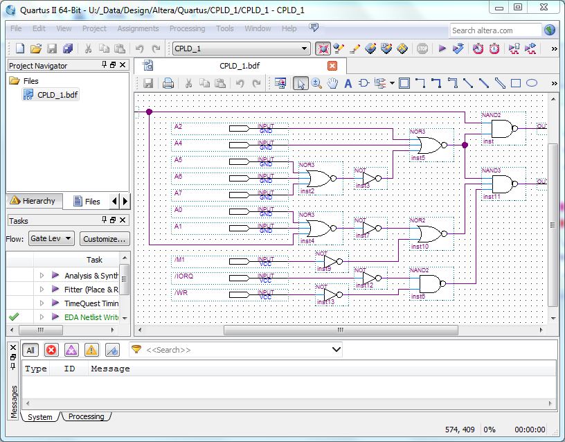
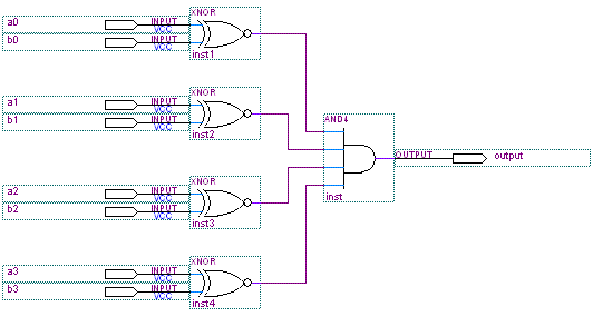
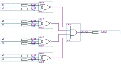
| A typical example of a small schematic
created using the Quartus II
schematic editor.
This is the easiest way to get started
designing for the CPLD - hence the reason I'm
using it ! |
 |
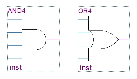
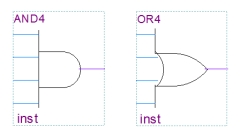
| Quartus II
includes a number of libraries of varying
complexity that can be used to implement the
required design At the most basic level, the
libraries include the basic logic gates such as
AND, OR, etc., as
well as a number of larger size gates that are
not normally available in hardware, such as 12
input NAND gates and the like. |
 |
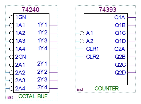
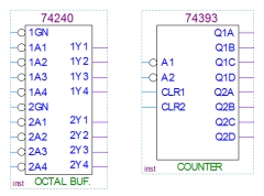
| Going a step beyond basic logic gates, Quartus II
also includes a library of standard 74 series
logic components, e.g., the 74xx240 and 74xx393
shown here. These function blocks make it very
easy to implement traditional logic designs
inside the CPLD. |
 |
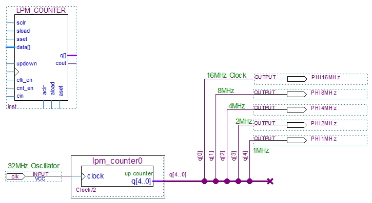
| Quartus II also includes a
large number of what Altera term "megafunctions",
To
quote from Altera, "Megafunctions are
ready-made, parameterized, pre-tested blocks of
intellectual property that are optimized to make
efficient use of the architecture of the
targeted programmable device."
The megafunction blocks include
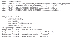
"Libraries of Parameterised Modules"
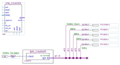
(LPM) such as the example shown of a LPM_COUNTER
module. When added to a schematic the module is
tailored to the application by adjusting the
appropriate parameters. |
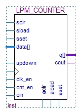 |
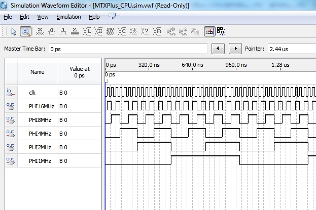
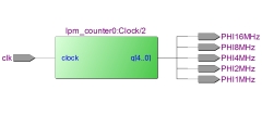
| This is an example of an LPM_COUNTER
instantiated in a schematic as lpm_counter0 with
the parameters set to create a 5-bit up counter.
It is used here to produce sub-clocks from a
32MHz source clock. NB: This example does not
confirm to Altrera's recommended design
practices, but it does illustrate the use of an
LPM. |
 |
|
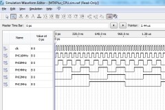
Functional Simulation |
| Once the design has been entered, the
circuit can be tested in functional
simulation. Test waveforms can be
entered and used to verify that operation of the
circuit is as intended. At this stage, there
may be timing issues that would prevent the
design from operating as intended once the
device timing limitations are taken into
account. |
 |
|
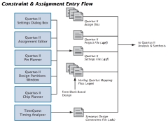
Constraints |
| Once the design has been entered, the
Assignments menu in the Settings
dialog can be used to specify initial design
constraints, such as pin assignments, device
options, logic options, and timing constraints.
By default, during compilation, Quartus
II is free to choose which pins on the
device are used for the inputs and outputs in
the design.
The TimeQuest analyzer
determines the timing relationships that must be
met for the design to correctly function, and
checks arrival times against required times to
verify timing. |
 |
|
Synthesis |
| Synthesis is the process of converting the
design into a circuit made up of the logic
elements (LEs) from the CPLD (or FGPA). |
 |
|
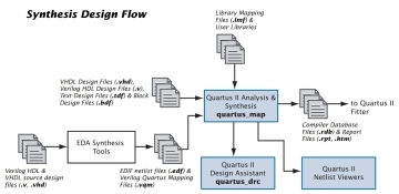 |
| The software optimizes the logic by
eliminating redundant terms and generating a
netlist, (a connection list) that is
a complete description of the circuit.
If required, the resultant netlist can be
exported in text form for use by other
EDA tools |
 |
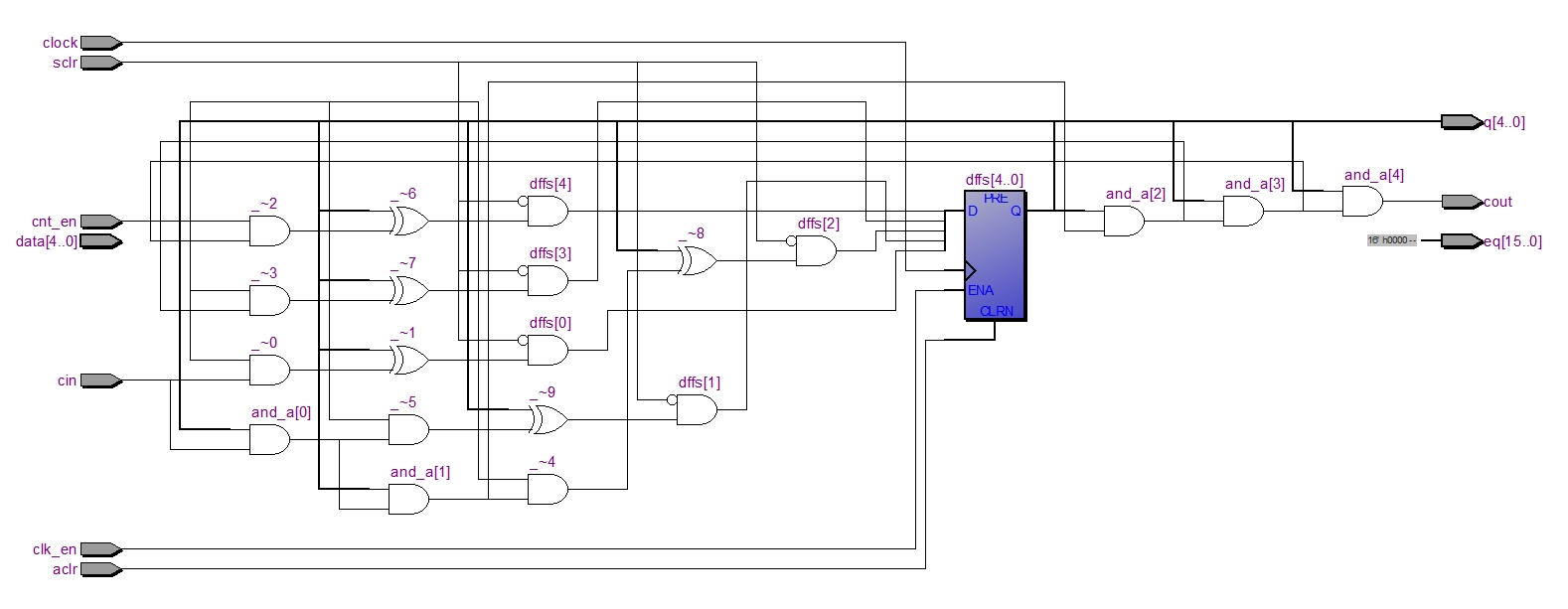
| Quartus II
includes a number of graphical netlist viewers,
including the RTL Viewer shown
here.
This is the top level netlist view of the
LPM_COUNTER seen earlier, used to generate a
number of sub-clocks from the source clock. |
 |
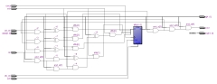
| By drilling down into the hierarchy, you can
see how the logic is produced from the
fundamental logic blocks, e.g., AND and OR gates
and flip-flops etc. |
 |
|
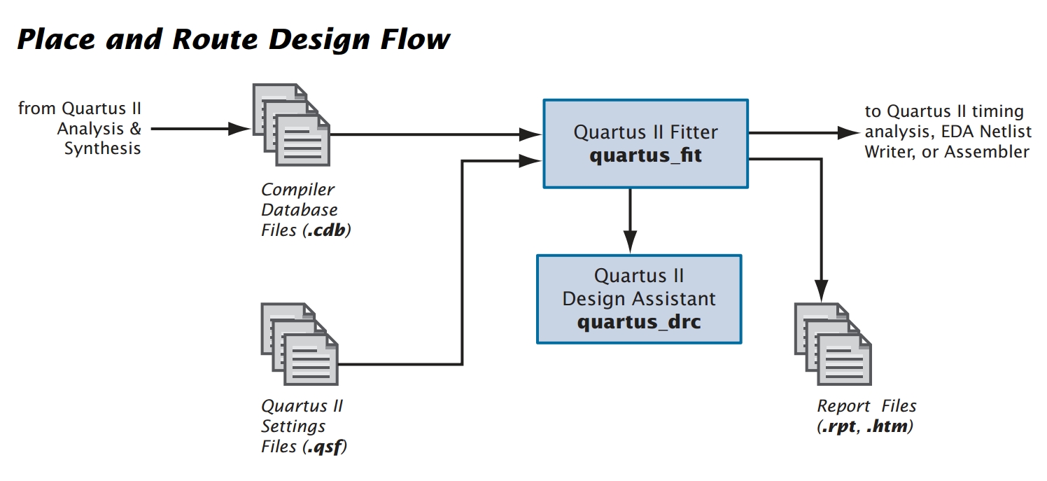
Place & Route |
|
The
next step is to map the netlist into the target
device using the Quartus II Fitter.
Using
the database that has been created by Analysis &
Synthesis, the Fitter matches the
logic and timing requirements of the project
with the available resources of the target
device. It assigns each logic function to the
best logic cell location for routing and timing,
and selects appropriate interconnection paths
and pin assignments.
 |
 |
|
Analyzing Fitting Results |
| Quartus II includes several
tools to aid in the analysis of the design
compilation and fitting phases. The Message
window and Report window provide fitting results
information. The Chip Planner
(shown) provides a GUI that allows you to view
the logic placement made by the fitter and/or
user assignments, lock regions of logic and view
routing congestion.
This condensed view, shows 4 LABs (A, B, C
and D) with LAB-A selected - indicated by the
blue frame. The four blocks to the left are the
reserved I/O pins - 1,2, 83 & 84 - in this case,
pin 83 assigned to the external clock (clk) |
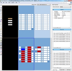 |
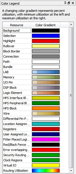
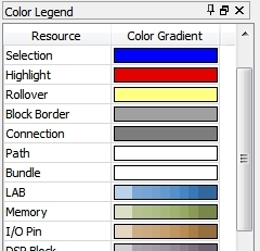
| Resource elements in the chip planner are
colour coded, the different colours representing
different resources such as pin assignment
status, logic cells etc. A changing colour
gradient represents percent utilisation, with
minimum utilisation at the left and maximum
utilisation at the right. In the image above,
the selected element is indicted by the blue
block with the details on the selected element
displayed in the right hand window.
The Chip Planner also allows you to view the
node fan-out and fan-in for specific structures,
or view the paths between specific nodes. |
 |
|
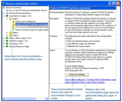
Fit Optimisation |
| Several Fit optimisation options are
available, including the Resource
Optimisation Adviser and the
Design Space Explorer |
 |
|
Timing
Analysis |
| The Quartus II TimeQuest
Timing Analyser is a static timing analyzer that
"validates the timing performance of all logic in your
design using an industry-standard constraint, analysis,
and reporting methodology. It supports the
industry-standard Synopsys® Design Constraints (SDC)
format." [See the
Altera TimeQuest resource page for more details]
My MAX7128S Timing
page gives a very brief overview of the timing
parameters applicable to the MAX7128S.
Using the constraints menu of
the TimeQuest
Timing Analyser, you can specify timing
constraints for elements of the design,
including I/O pins, clock settings, I/O delays.
Once the initial timing analysis is complete,
timing simulations are performed on the design
to ensure that there are no problems due to the
specific delays in the target device. |
 |
|
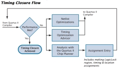
Timing Closure |
| The Timing Closure flow
optimises the timing to meet the timing goals by
controlling the
Synthesis and
Place & Route
functions. |
 |
|
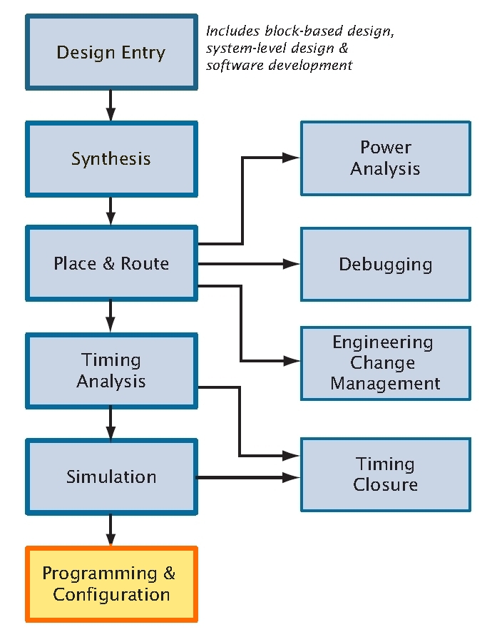
Programming
& Configuration |
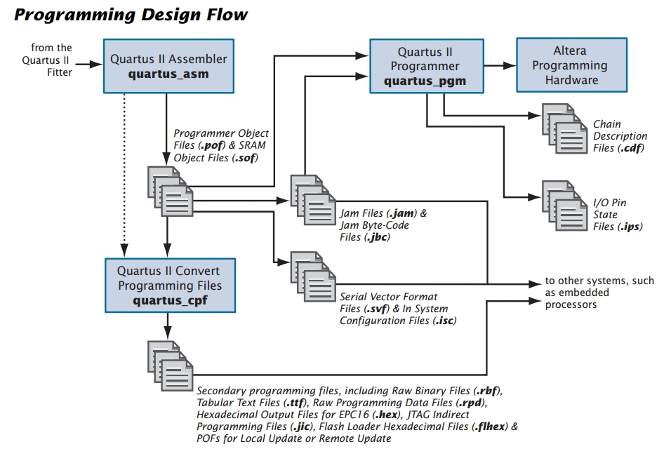
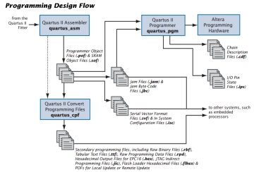
| The Quartus II Assembler
module generates programming files that are
downloaded to the device using the appropriate
Altera programming hardare - in this case, the
USB Blaster.
 |
 |
| When a design is successfully compiled, the
Fitter's device, logic cell and
pin assignments are converted into a programming
image that can be loaded to the device. The
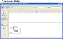
Programmer option is accessed from the Quartus II
Tools
menu option from where the program is downloaded
to the target device |
 |
|
Quartus II
Resources
For comprehensive
instructions, help and training materials, refer
to the
Quartus II Documentation page on the Altera
website. |
| Title |
Publisher |
|
Quartus II Handbook - Version
13.1, QII5V1-13.1.0, November 2013 |
|
3 Volumes, 1681 Pages, 38 MB PDF |
|
|
Volume 1:
Design and Synthesis (890 pages) |
| |
Volume 2:
Design Implementation and
Optimization ( 299 pages) |
| |
Volume 3:
Verification (402 pages) |
|
Altera |
|
|
|
|
Introduction to Quartus II Software -
Version 1.0, May 2011
The product sales brochure, gives a very high
level overview |
Altera
|
|
Quick Start Guide for Quartus II Software
-Version 7.2, Oct 2007 |
Altera |
|
LPM Quick Reference Guide - December 1996 |
Altera |
|
Integer Arithmetic Megafunctions User Guide
- UG-01063 - June 2010 |
Altera |
|
TimeQuest Timing Analyser - QII53018-13.1.0
- November 2013 |
Altera |
|
The TimeQuest Timing Analyser Quick Start
Tutorial - December 2009 |
Altera |
|
The TimeQuest Cookbook - MNL-01035-1.3 -
January 2011 |
Altera |
|
Timing Analysis Overview - QII53030-12.0.0 -
June 2012 (Version 12) |
Altera |
|
Timing Analysis Overview - QII53030-14.0.0 -
June 2012 (Version 14) |
Altera |
| |
|
|
Altera Training Materials |
|
|
Quartus II Basic Training, PowerPoint
Presentation from 2005 |
Altera |
|
Quartus II Software Design Series : Foundation
from 2008 |
Altera |
| |
|
MAX7128S Timing <
Previous
Page Goto
Next
Page >
MAX7128S Programming
|