|
"MTX Plus+" CPU Board (Version 2.3)
Overview
My original design for the CPU
board was based on the use of discrete logic chips, like the
original MTX. The design was more or less finalised when I
decided to use a
CPLD in the design to reduce the congestion on the somewhat
cluttered circuit board and to make it easier to modify the
glue logic
should any changes be necessary.
The Wikipedia entry for
CPLDs uses a photo of an Altera EPM7128S as an example of a
typical CPLD. Coincidentally, Lez Anderson had included this
device in the bag of "free stuff" that he generously sent me
when the MTXPlus+ project was first mooted, so this seemed like an
obvious device to use. Given that I have absolutely no knowledge
of using and programming a CPLD, this will delay the production
of a working CPU board but will, hopefully, lead to a better
design.
The other advantage of using an Altera device is that I
already had a very basic introduction to Altera's
Quartus II Web Edition software when I loaded the software
for Andy Key's
REMEMOTECH project onto my Altera DE1 development board as
described on the
My REMEMOTECH
page. That page also describes how to obtain a copy of this free
software from the Altera web site.
| Altera EPM7128S
Abridged Specifications (PLCC) |
| |
|
| Useable logic gates |
2,500 |
| Macrocells |
128 |
| Logic array blocks |
8 |
| User I/O pins |
68 |
The basic specifications of the EPM7128S are shown in the
table, for more detailed information on this CPLD and my
attempts to use it can be found on
my CPLD page.
The Version 2 CPU board uses
a Z80 CPU in a DIP-40 package and the
Version 3 board uses a Z8S180
CPU in a PLCC-68 package.
Hardware - Control Bus Signals
The backplane distributes a number of control signals to the
rest of the boards in the system, the majority of these are
standard Z80 control bus signals, generated by the CPU, but
there are also a number of other signals generated or used on
the CPU board that are distributed over the backplane. The
source of some of these signals differs between Version 2 and
Version 3 of the CPU board.
| Name |
Description |
Source |
Direction |
| Clock |
Clock source for the CPLD |
X1 |
To CPLD |
| PHI4 |
4MHz clock signal |
CPLD (v2)
or X2 (v3) |
To Backplane |
| PHI |
System
clock signal
|
CPLD (v2)
or CPU (v3) |
To Backplane |
| PHI8 |
Additional 8MHz clock signal |
(Deleted) |
(Deleted) |
| SER01 |
Clock for serial port 1 |
CTC |
To Backplane |
| SER02 |
Clock for serial port 2 |
CTC |
To Backplane |
| DIAG |
Signal to the Diagnostic board to
latch 7-segment displays based on logic in the CPLD.
By reprogramming the CPLD and switching the position
of jumper J5, simple on board status conditions can
be shown using the on board "DEBUG" LED. |
CPLD |
To Diag.
board |
| /VDPINT |
Interrupt signal from VDP |
VDP |
From Video
board |
Hardware - Real Time Clock Sub-system
The CPU board includes an RTC using the Dallas
DS12887 that Lez included in his "kit of parts".
As described on my
Notes page, I found this really
helpful article written by a Wilf Rigter around 1996. The
article demonstrates the use of the DS1287 (an earlier version
of the DS12882) with a ZX81 and included examples of Z80
assembler and BASIC programs to access the chip. Martin was able
to use this information with the DS12887 and modified address
decode logic to make a working RTC that will be included on the
MTXPlus+ CPU board and has posted the details on the Memotech
forum in
this thread.
Status Summary
Development of the Version 2
and Version 3 CPU boards
are described in more detail on their own pages. The Version
2 board had pretty much been proven to
meet original design intent for MTX compatibility - at
least, when running at 4MHz like the original. However, as
things progressed during the build, a number of changes were
made to correct a couple of weaknesses in my design. Added
to this was some degree of "scope creep" that led to other
modifications and enhancements. These "design
developments" were originally documented on this page, but
the number and magnitude of the changes probably justifies
their description on a separate page that I've called, oddly
enough, Design Development.
The main items are now just bulleted below, for details of
the changes, click on the links to open the new page.
In addition to the enhancements to the
Version 2 Z80 board, an enhanced board, based on the Z8S180
is currently in development.
Design Development
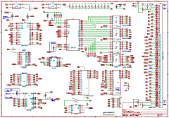
Version
2.21 of the CPU board design, this version of the board
was used to prove the base functionality of the system
and test development of the more advanced features.
This version incorporates TTL buffer chips on the
Z80 Address, Data and Control lines that were not
required and removed from the final design. |
 |
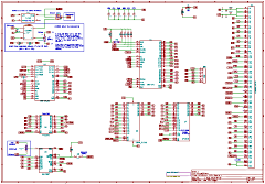
The "final"
version of the Z80 board used to produce the CPU PCB.
This version incorporates the "Mystery" upgrade, and
due to its increased complexity, no longer includes the
option to implement the glue logic in GALs; the board is
based on a CPLD only solution. |
 |
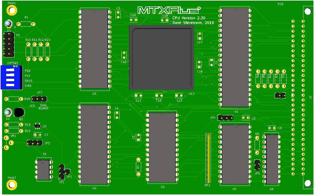
| The KiCAD
3D model of the Z80 CPU PCB |
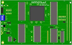 |
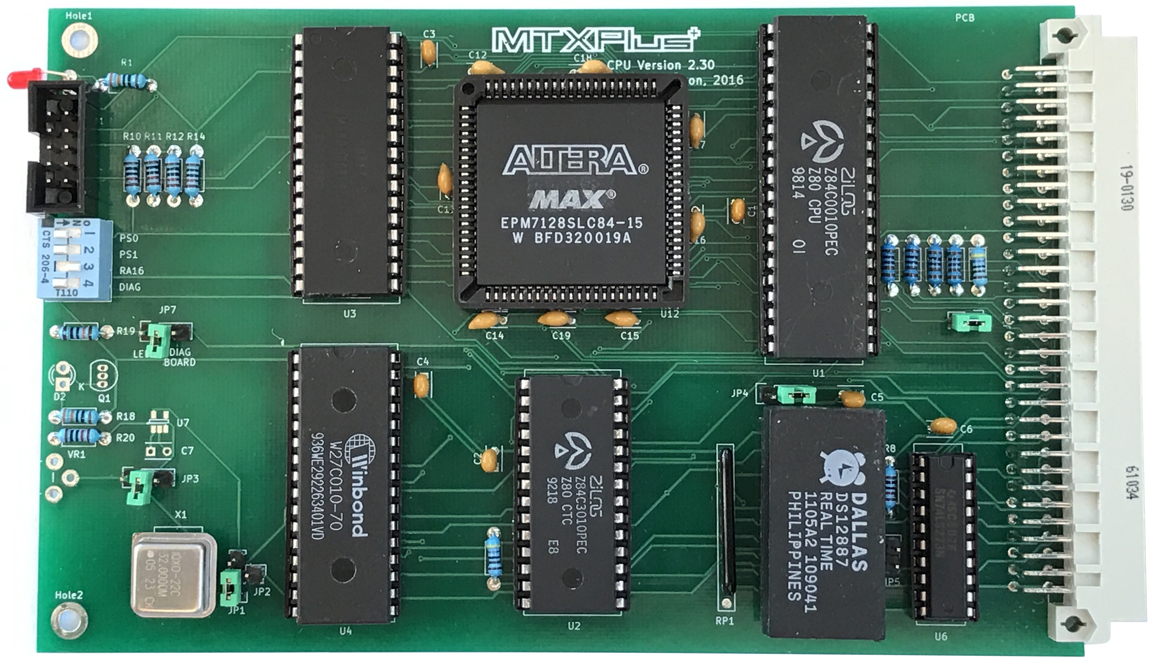
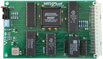
The
assembled PCB
I seem to be getting better - just
one minor routing error on this one! |
 |
|