|
"MTX Plus+" CPU Board -
CPLD

Having abandoned the idea of using discrete 74LS00 series
logic, the CPU board design will now be based around a
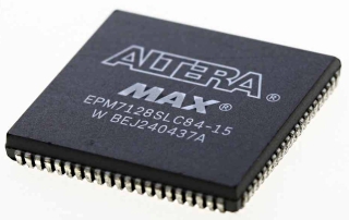
CPLD - the Altera
EPM7128SLC84. Using this chip may seem a strange
choice, so it probably warrants some explanation. A comparison
of the pros and cons in the table below may help. This is
obviously very subjective and only really relevant to
the specific case of my CPU board.
| Advantages |
Disadvantages |
| Availability |
Lez Anderson included
this device in the bag of "free
stuff" that he sent me |
| |
They are also readily
available from ebay sellers, in the UK,
the Far East. etc. |
|
| Age |
The MAX7000S series was
introduced in 1995, much newer, smaller
devices are available |
|
| Price |
Apart from the obvious
price benefit noted above : |
| |
they are relatively low
cost, depending on the speed, costing anywhere
from £20 to £50 |
|
| Footprint |
The EPM7128SLC84 is in
an 84 pin
PLCC package. Compatible sockets to
allow through hole PCB mounting are
~37mm square. This is quite a large area
but is offset by the number of discrete
logic chips that a CPLD can replace. |
|
| Power |
For my application, with
2,500 logic gates and up to 64 I/O pins
available, it is certainly
powerful enough. * |
|
| Power |
Overkill? The relatively
high capacity comes with the footprint
penalty noted above. A smaller footprint
would be an advantage. * |
|
|
|
| Software + |
Quartus II is the
development tool for the full range of
Altera
FPGAs and CPLDs, it will take some
time to become familiar with it before
the design can progress. |
|
So, you may disagree with my choice
of CPLD, but for the reasons given, the decision is
made. At the point that this decisions was taken, I
had little knowledge and no experience of CPLDs, so
time may tell whether I should have made a different
choice.
*As it turns out, the CPLD is doing a
lot more than I first envisaged, as well as the
basic functions such as the ROM/RAM decode logic,
memory and I/O chip selects and simple clock
division, it is now at the heart of the
implementation of
Speculator+ on MTXPlus+.
The EPM7128 is now pretty much full to capacity and
the system may have benefited from a CPLD with even
more capacity.
+ Many of
the current logic chip manufacturers supply FREE
development environments to support their products,
the facilities available in the free versions of the
tools vary though.
Altera seem to be one of the most generous with
their tools - the free Web Edition of
Quartus II supports various options such as
schematic entry and VHDL/Verilog programming. It
also provides functional and timing simulation.
I believe that the
Xilinx (ISE)
and
Lattice (ispLever)
tools provide similar functionality in the free
versions of their development tools.
Atmel
is much less free with their
ProChip Designer tool, the free version only
provides very limited functionality, i.e., no
schematic entry or simulation tools. Although Atmel
make an unrestricted version of
WinCUPL available, it has very limited
functionality. So, while the hardware might be
cheap, the Atmel products are much less useful for
the hobbyist. |
| Altera EPM7128SLC84
Abridged Specifications |
|
The
MAX7000 datasheet is available |
| Useable logic gates |
2,500 |
| Macrocells |
128 |
| Logic array blocks |
8 |
| User I/O pins |
68 |
| The "S" denotes that the device is "in-system"
programmable, by including a 4-pin
JTAG interface
on the PCB, which requires 4 I/O pins, the device can be programmed in situ,
without a requirement for an external programmer. |
| The "LC84" suffix denotes that the
CPLD is packaged in 84 pin PLCC |
| The speed rating of the chip is
appended to the part number to indicate the pin-pin
delay of the part, e.g., an EPM7128SLC44-12 denotes
a pin-pin delay of 12ns. Available speeds are 5, 6,
7, 10, 12, 15 and 20ns. |
Detailed specifications and an overview of its operation can
be found in the
MAX7000
datasheet. On the next pages I will give a basic introduction
to the EPM7128S, based on the knowledge that I acquire as
I learn how to produce the CPLD design
for MTXPlus.
CPU
Board Overview <
Previous
Page Goto
Next
Page >
PLD Basics
|