|
"MTX Plus+" -
I/O Port Allocation
Introduction
This page provides details of the I/O port allocation for
MTXPlus+, details of the I/O board
itself can be found on its own page.
To retain software compatibility with the original MTX
design, the upgraded system will need to be I/O port and
graphics compatible with the MTX, but will also be capable of
operating in an enhanced configuration with a higher processor
speed, more memory and enhanced graphics capabilities.
|
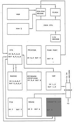
MTX I/O Port Allocation
This block diagram is from the
MTX
Operator's Guide and gives a high level overview
of the MTX design, including the I/O port
allocation.
The vast majority of information on this page is
available in the MTX Operator's Guide but I will
document the port allocation here, if for no other
reason than to make sure that I understand it as I
design MTXPlus+.
The cassette interface is shown in
grey and will not be used in MTXPlus. Other than to
maintain full compatibility with the MTX, there is
no real justification for including cassette data
storage - floppy disk and/or memory card storage
will be added in due course.
I would also like to do away
with the TV interface and upgrade the graphics
output from the VDP to VGA, this is more challenging
though, as I have not found a simple way of building
a scan doubler. The only options at the moment would
seem to be to use an "off-the-shelf" external
converter like the
one that
I use with my FDX, or to go for an (expensive)
FPGA solution.
|
 |
|
Draft I/O Port Allocation for
MTXPlus+ |
|
|
|
I/O Port
Decode Logic
As the original MTX was a single
board computer, the I/O port decode logic for all of
the ports on the motherboard (0 to B) was on the
motherboard itself. Since the
I/O functions were going to be distributed over a number of different boards, the
option for MTXPlus was either to keep all of the logic on the
CPU board and use the bus to distribute the port
select signals, or to build only a subset of the
decode logic on both the CPU and the I/O boards as required.
The first option would have reduced
the amount of repeated logic and consequently, the
number of chips required, but would have meant that
additional bus signals were required that would only
be used on a single I/O board. The original plan was
for the CPU board to include I/O port decode logic
only for ports actually on the board. The
decision to use a relatively powerful CPLD for the
glue logic makes a considerable quantity of
additional logic capability available on the CPU
board and I did consider doing the majority of the I/O port
decode logic on the CPU board, but, because of the
limited number of backplane signals, I chose to
stick with the original plan and only decode the I/O
ports actually on the CPU board, i.e., the Page Port
(OUT0), the CTC ports (08-0Bh) and the MTXPlus+ RTC
ports, (70 & 71h). |
|
MTX Original I/O Ports |
|
Page Port
(Out 0)
The MTX
"Page Port" probably deserves a mention here, it is
fundamental to understanding how the MTX could
support more than 64k of memory and how MTXPlus+
memory paging will work to retain compatibility with
the MTX.
The Z80
has a 16 bit address bus and can therefore address 216
memory (or I/O) locations at one time, i.e., 65536
memory addresses. Using
bank switching, different pages of physical
memory can be switched in and out of the address
space.
In the
MTX, the Page Port, (Output Port 0),
is used to control memory addressing, MTX could
operate in either a ROM based or a RAM based mode.
Page Port Structure
|
Bit |
D7 |
D6 |
D5 |
D4 |
D3 |
D2 |
D1 |
D0 |
|
Function |
RELCPMH |
R2 |
R1 |
R0 |
P3 |
P2 |
P1 |
P0 |
|
|
Mode |
ROM |
RAM |
Bits D0
to D3 (P0 to P3) define the RAM page address
Bits D4
to D6 (R0 to R2) define the ROM page address
Bit D7 (RELCPMH)
defines a ROM based system (D7 = 0) or a RAM based
system (D7 = 1)
[Andy has
advised that the meaning of the acronym for bit 7 is Rom
Enable if Low, CP / M if
High.]
The MTX RAM map had a block of memory from C000h to
FFFFh (4000h, 16k bytes) that was common between all of the
available RAM pages, this allowed bits P0, P1, P2
and P3 to select one of the 16 possible pages of
48k, this gives the MTX a maximum addressable memory
of (16 * 48) + 16 = 784K.
In the original MTX, the additional memory above 64k
was not available to MTX BASIC and was typically
used to configure a RAM disk.
Since the maximum RAM disk size supported by the MTX
was 512k, the largest useable memory configuration
was with 64k on board and an additional memory
expansion card of 512k, either internal to the MTX
or as part of the SDX disk controller.
Memory mapping in MTXPlus+ has been improved over
the Memotech original and, if not used for other
purposes, 448k is available for use from MTX BASIC. |
|
Video Display
Processor Ports (In 1&2, Out 1&2)
The TMS 9918/29 VDP in the MTX uses
two ports :
| VDP
Port |
Dir |
VDP
Function |
MTX
Port |
Dir |
|
0 |
In/Out |
VRAM Data |
1 |
Out/In |
|
1 |
In |
Set up
data port address register |
2 |
Out |
| Write to VDP Register |
| Out |
Read from VDP
Register |
In |
The VDP for MTXPlus is to be the
Yamaha V9958, it is software compatible TMS9918A
and V9938. Control of the additional features of
the V9958 requires 4 ports. The ports used in
the MSX2 computer are shown for reference, the
I/O port allocation for the MTXPlus VDP has not
been finalised
| VDP
Port |
Dir |
VDP
Function |
MSX
Port |
Dir |
|
0 |
In/Out |
VRAM Data |
98h |
Out/In |
|
1 |
In |
Set up
data port address register |
99h |
Out |
| Write to VDP Register |
| Out |
Read from VDP
Register |
In |
| 2 |
In |
Palette
Registers |
9Ah |
Out |
|
3 |
In |
Register Indirect Addressing |
9Bh |
Out |
| Out |
In |
|
|
Sound Port
(In 3, Out 6)
The MTX used a Texas Instruments SN76489 Complex
Sound Generator interfaced using I/O ports 3 (IN)
and 6 (OUT). MTXPlus+ will use the same system, with
the sound chip and associated '374 octal "D" type
flip-flop being installed on the video board.
IN(3) is used as an output strobe into
the sound generator. After data has been latched
into the output port (6), data may be immediately
strobed in using this line. A total of at least 32
clock cycles must have elapsed before additional
data may be strobed using IN(3).
OUT( 6 ),d is used to provide latched
data for the sound generator which is subsequently
strobed using IN(3). |
|
Parallel
Printer Port (In 0, In/Out 4)
The MTX supported the use of a
Centronics parallel printer interfaced through I/O
ports 0 (IN only) and 4 (IN/OUT). For simplicity,
MTXPlus+ will use the same system in the base
design. although consideration will be given to
developing a USB solution for enhanced functionality
with the MTXPlus+ enhanced mode.
In the MTX ROM, IN(0) is used to set
the active low printer STROBE line LOW
to signal the data is ready to be sent to the
printer.
|
IN(4),d is used to monitor the
status of the printer port |
|
D0 |
BUSY |
Handshake line |
Active high |
|
D1 |
ERROR |
|
Active low |
|
D2 |
PE |
Paper
Empty |
Active high |
|
D3 |
SLCT |
Printer in selected state |
Active high |
OUT( 4),d is used to send data to the
printer. Valid data should be latched into this
port. When status on IN( 4) reads not
BUSY and selected, then data should be strobed after
a delay of approximately 1 microsecond using
IN(O) to force STROBE low. After a further
delay of approximately l microsecond STROBE
should be forced high using IN( 4). |
|
Keyboard
& Joystick Ports (In 5 & 6, Out 5)
Memotech computers used a very basic
matrix keyboard, the keyboard was connected to the
computer board by a number of drive and
sense lines, controlled/read through I/O ports 5
& 6. More details of the original design are
described are described on my
MTX computer keyboard page. Joysticks in the MTX
were wired in parallel with keys on the keyboard and
did not require any additional hardware or logic to
use them.
When new, the MTX keyboard was
probably the best keyboard of any of the home
computers of the time, given their age now though,
the keyboards are prone to sticky and repeating keys
and a new keyboard is really needed for MTXPlus. The
most readily available and cheapest keyboards are PC
PS/2 or
USB
keyboards, both of these would require an interface
to be built, but I think that the simpler of the two
is the PS/2 option, so, MTXPlus+ will eventually
have a PS/2 keyboard attached.
The link between a PC and PS/2
keyboard is a serial one, the keyboard sends scan
codes to the PC which are usually decoded by a
microcontroller on the motherboard. Whilst the
concept is straightforward, it may take a little
time to design and build a suitable interface, to
allow MTXPlus+ to become useable while a PS/2
interface is being developed, a "temporary"
interface, using the same logic as the MTX, will be
included to allow connection of an original MTX
keyboard.
In the MTX ROM :
IN(5),d is used to read the least
significant 8 bits from the ten bit sense line of
the 8 x 10 keyboard matrix.
IN( 6 ),d is used to read in the two
most significant sense lines (DO and D l) of the 8 x
10 keyboard matrix.
The two bit country code switch is read on D2 and D3
of this port.
OUT(5),d is a latched port that
provides the 8 drive lines of the 8 x 10 keyboard
matrix.
|
|
Uncommitted Parallel Input /
Output port (PIO)
IN(7),d
This is the input port for the uncommitted
parallel input output port (PIO). Data may be
latched in for reading with an active low pulse on
the enable line, designated INSTB.
OUT(7),d
This is the output port of the PIO. It is a
latched output with tri-state output control using
ONSTB.
This port will
not be used in MTXPlus+ |
|
Counter/Timer Ports (In & Out,
8, 9, A, B)
The CTC will be included on the CPU
board and will use the same logic as the MTX board.
On the MTX circuit diagram, the CE
signal to the CTC is referred to as
PE8T11, to convey Port Enable 8 to 11
(08 - 0Bh). These are four contiguous
read/write ports for the four channels of the Z80A
CTC.
| Port |
Target |
Input |
Output |
| 08 |
Channel 0 |
VDPINT |
(no connect) |
| 09 |
Channel 1 |
4MHz/l3 Clock
(307kHz clock for DART) |
DART serial clock 0 (SER01) |
| 0A |
Channel 2 |
DART serial clock 1 (SER02) |
| 0B |
Channel 3 |
RTC
Int
(MTX Cassette )
|
(not available on CTC) |
In the original MTX, the CTC Channel
0 output was not used and the Channel 3 input was
used by the MTX cassette tape interface. These
channels are reused in MTX Plus+ to
provide an automatic way for the system to calibrate
time dependent ROM functions such as cursor flash
and keyboard repeat based on the chosen CPU clock
rate. This functionality is described in more detail
on the ROM
timing page. |
|
Serial Ports (In & Out,
C, D, E & F)
|
Port |
Target |
|
0C |
RS232-A Data |
|
0D |
RS232-B Data |
|
0E |
RS232-A Control |
|
0F |
RS232-B Control |
On the MTX, I/O channels 0C to 0F are used for
the two RS232 ports, implemented using a Z80A DART.
The DART must be clocked at the same frequency as
the CPU, this was fine for the 4MHz MTX, as the DART
is available in NMOS versions with maximum clock
speeds up to 6MHz.
For MTXPlus+, the Z80 DART will be replaced with
the more versatile Z80 SIO. CMOS versions of the SIO
are available with clock speeds up to 10MHz, still
below the intended clock rate (16MHz) of the
computer, but, the encouraging results that we have
seen with over-clocking CMOS Z80 CPUs made us
optimistic that a 10MHz SIO would be reliable at
16MHz - time will tell! |
| |
|
|
Additional I/O Ports |
In the original Memotech computer, Port 1F was
reserved to support remote control of the cassette
motor for loading and saving to tape.
In the
Sinclair Spectrum, port 1F was used by the Kempston
Joystick interface; this interface did not just map
to keys on the Spectrum keyboard as most other
joystick interfaces did, it required that games
included specific code to interface with I/O Port 1F
in order to support the Kempston joystick interface.
The original version of
Memotech Speculator used Port 1F to support the
Kempston Interface, mapping the MTX keyboard presses
and the equivalent Memotech Joystick feedback to the
Kempston equivalents. MTXPlus+ uses this port in the
same way to support Speculator+.
|
Bit |
Function |
Description |
|
0 |
Right |
Button pressed (Active Low)
In/Out |
|
1 |
Left |
Button Pressed (Active Low)
In/Out |
|
2 |
Down |
Button Pressed (Active Low)
In/Out |
|
3 |
Up |
Button
Pressed (Active Low) In/Out |
|
4 |
Fire |
Button
Pressed (Active Low) In/Out |
|
5 |
(none) |
Not Used
- bit returns xx0 to IN (1F) |
|
6 |
(none |
Not Used
- bit returns x0x to IN (1F) |
|
7 |
(none) |
Not Used
- bit returns 0xx to IN (1F) |
|
|
8255
Peripheral Interface Adapter (In & Out, 6C, 6D, 6E
& 6F)
|
Port |
Target |
|
6C |
8255 Port A |
|
6D |
8255 Port B |
|
6E |
8255 Port C |
|
6F |
8255 Control Word |
The 8255 PPI has 3 x 8-bit data ports which may
be configured in various modes using the control
word. For MTXPlus+, the PPI will be used to provide
an IDE/Compact Flash interface, ports A and B will
form the 16 bit data word for the IDE/CF bus and
port C will be used for the control signals. The
8255 port allocation for MTXPlus+ was originally
60-63 but was changed to make them consistent with
CFX, which doesn't
have enough logic gates to decode ports 60-63.
|
IDE/CF Control Signals on
8255 Port C |
|
Bit |
Function |
Description |
|
0 |
DA0 |
Device Address 0 |
|
1 |
DA1 |
Device Address 1 |
|
2 |
DA2 |
Device Address 2 |
|
3 |
CS0 |
Chip Select 0 |
(Device Registers 0-7) |
|
4 |
CS1 |
Chip Select 1 |
(Device Registers 8-15) |
|
5 |
DIOW |
Write Select |
|
6 |
DIOR |
Read Select |
|
7 |
RESET |
Device Hardware
Reset |
The 8255 PPI was developed by
Intel, an
interesting Q&A article is available in the
Intel archive on their website. There is an
interesting article about using IDE with a Z80
on the
retroleum.co.uk website |
Real Time
Clock
The RTC is a Dallas DS12887 - a
drop in replacement for the RTC in an IBM/AT and
will use the same I/O ports as the IBM to make cross
referencing IBM documentation easier.
The RTC is accessed using MTXPlus+ I/O ports 70h
(112d) and 71h (113d).
A write to Port 112 sets up the address in the
RTC memory map and a subsequent read or write to
port 113 reads or sets the data in the RTC
register.
|
Port |
Dir |
Function |
|
70 |
Out |
CMOS RAM index register port
Bits 0-6 Index into 128 bytes of
non-volatile RAM
(Bit 7 Not used in MTXPlus) |
|
71 |
In/Out |
RTC registers:
| Dec |
Hex |
Description |
Range |
|
00 |
00 |
Current
Second |
00 - 59 |
|
01 |
01 |
Seconds
Alarm |
00 - 59 |
|
02 |
02 |
Current
Minute |
00 - 59 |
|
03 |
03 |
Minutes
Alarm |
00 - 59 |
|
04 |
04 |
Current Hour |
00 - 23 |
|
05 |
05 |
Hours Alarm |
00 - 23 |
|
06 |
06 |
Day of the
week (Sunday = 1) |
01 - 07 |
|
07 |
07 |
Date of the
month |
01 - 31 |
|
08 |
08 |
Month |
01 - 12 |
|
09 |
09 |
Year |
00 - 99 |
|
10 |
0A |
Status
register A (Bit 7 is Read
only) |
|
|
11 |
0B |
Status
register B |
|
|
12 |
0C |
Status
register C (Read only) |
|
|
13 |
0D |
Status
register D (Read only) |
|
|
14 |
0E |
The
remaining 114 general
purpose non-volatile
registers are available for
custom use |
0 |
|
to |
to |
|
127 |
7F |
255 |
For a full description of the registers
and status bytes, see the Dallas
Semiconductor
DS12887
datasheet
Non-Volatile RAM
A number of the RTC NVRAM registers are
used to store MTXPlus+ configuration data in a
similar way as the CMOS RAM was used in an IBM PC.
| Dec |
Hex |
Description |
Range |
|
16 |
10 |
Default CPU
Speed (see the
clocks page) |
00 - 15 |
|
17 |
11 |
SDX Boot
Drive
B (00), C (01), D
(10), E (11) |
00 - 03 |
|
18 |
12 |
BASIC Text
Colour Attributes |
00 - 255 |
|
19 |
13 |
PANEL Text
Colour Attributes |
00 - 255 |
|
20 |
14 |
NTSC (0) or
PAL (2) |
00 - 02 |
|
21 |
15 |
RAM Pages
for BASIC |
00 - 13 |
|
22 |
16 |
Mono CP/M
Text Colour Attributes |
00 - 255 |
|
... |
... |
(Not used) |
|
|
127 |
7F |
RTC CMOS CRC |
00 - 255 |
|
The text colour registers
store the screen attributes
for text modes in the same
way as VDP status register
7, i.e., the upper 4 bits
contain the colour code of
colour 1 (foreground) and
the lower 4 bits contain the
colour code of colour 0
(background). |
|
0 |
0 |
Transparent |
|
|
1 |
1 |
Black |
|
|
2 |
2 |
Medium Green |
|
|
3 |
3 |
Light Green |
|
|
4 |
4 |
Dark Blue |
|
|
5 |
5 |
Light Blue |
|
|
6 |
6 |
Dark Red |
|
|
7 |
7 |
Cyan |
|
|
8 |
8 |
Medium Red |
|
|
9 |
9 |
Light Red |
|
|
10 |
A |
Dark Yellow |
|
|
11 |
B |
Light Yellow |
|
|
12 |
C |
Dark Green |
|
|
13 |
D |
Magenta |
|
|
14 |
E |
Grey |
|
|
15 |
F |
White |
|
|
Examples |
Dark Green
on Black = 1100 + 0001
=
27 + 26
+ 20 = 128 + 64 +
1 = 193 |
|
|
|
|
Black on
Dark Green = 0001 + 1100
= 24 + 23
+ 22 = 16 + 8 + 4
= 28 |
|
|
|
|
|
|
|
|
|
|
|
|
|
|
|
|
|
|
|
|
|
|
|
|
|
|
|
|
|
|
|
|
|
|
|
|
|
|
|
|
|
|
|
|
|
|
|
Date & Time Functions
|
The time, date and alarm registers are
setup by the MTXPlus+ ROM to use binary
mode so all reads and writes from/to
these registers from MTX BASIC need to
be converted to the decimal equivalent
of the RTC register value.
|
For example, if the RTC is
operating in 24 hour mode
(controlled by Status Register
B, bit 1), to set the time value
to 19:20:05, the user could
write the decimal equivalent of
19h (25d),
20h (32d)
and 5h (5d)
to the appropriate RTC
registers. |
OUT 112,
4 |
Hours |
| OUT 113,
25 |
|
| OUT 112,
2 |
Minutes |
| OUT 113,
32 |
|
| OUT 112,
0 |
Seconds |
| OUT 113,
5 |
|
To simplify communication with
the RTC, additional commands
have been added to MTXPlus+
BASIC.
|
Set RTC Date & Time |
| USER
SETDATE |
"dd/mmyy" |
| USER
SETTIME |
"hh:mm:ss" |
|
Read RTC Date & Time |
| USER
GETDATE |
|
| USER
GETTIME |
|
|
Update MTX Clock from
RTC |
| USER
SETCLOCK |
|
|
Slow CPU Clock Source
For diagnostic purposes, it is possible
to run MTXPlus+ with an ultra-slow CPU
clock, this is derived from the Square
Wave Output of the RTC and can be set to
a range of values between 2Hz and 8,192
kHz, defined by the lower 4 bits of
Status Register A. (These bits also
setup the periodic interrupt rate to
generate a CPU interrupt for user
programs - this function is not used in
MTXPlus+).
Note:
Even at the maximum rate of 8Khz, the
slow clock is unlikely to be useful if
the only method of monitoring the system
is the video board. The system would be
running some 500 times slower than
design and take far too long to display
meaningful output to the screen. The
slow clock in designed to be used in
tandem with the Bus Diagnostic Card,
probably with a clock setting of 2
or 4 Hz.
| Status
Register A |
| Bit7 |
Bit6 |
Bit5 |
Bit4 |
Bit3 |
Bit2 |
Bit1 |
Bit0 |
| UIP |
DV2 |
DV1 |
DV0 |
RS3 |
RS2 |
RS1 |
RS0 |
|
|
Status Register A |
Periodic
Interrupt Rate |
SQW
Frequency |
|
RS3 |
RS2 |
RS1 |
RS0 |
|
0 |
0 |
0 |
0 |
None |
None |
|
0 |
0 |
0 |
1 |
3.90625
ms |
256 Hz |
|
0 |
0 |
1 |
0 |
7.8125
ms |
128 Hz |
|
0 |
0 |
1 |
1 |
122.070
us |
8.192
kHz |
|
0 |
1 |
0 |
0 |
244.141
us |
4.096
kHz |
|
. . . |
See
DS12887
datasheet for intermediate values |
. . . |
|
1 |
1 |
0 |
0 |
62.5 ms |
16 Hz |
|
1 |
1 |
0 |
1 |
125 ms |
8 Hz |
|
1 |
1 |
1 |
0 |
250 ms |
4 Hz |
|
1 |
1 |
1 |
1 |
500 ms |
2 Hz |
Status Register A is also used
to start & stop the RTC and
stores a flag (bit 7, read only)
signifying when an update will
soon occur (Update
In Progress).
To update the status
register, the a pattern of "010"
should also be written to bits
6..4 to ensure that the RTC is
running. For example, to set a
4Hz SQW frequency, a bit pattern
of x0101110 should be set (46d) |
Setup write to Register A |
| OUT 112,
10 |
|
Update SQW frequency bits |
| OUT 113,
46 |
| |
| |
|
| Status
Register B |
| Bit7 |
Bit6 |
Bit5 |
Bit4 |
Bit3 |
Bit2 |
Bit1 |
Bit0 |
| SET |
PIE |
AIE |
UIE |
SQWE |
DM |
24/12 |
DSE |
| SET |
0 when normal updates are
occurring, 1 when setting
date/time |
| PIE |
Periodic
Interrupt Enable (1 = enabled),
not used in MTXPlus+ |
| AIE |
Alarm
Interrupt Enable (1 = enabled),
not used in MTXPlus+ |
| UIE |
Update
Ended Interrupt Enable (1 =
enabled), not used in MTXPlus+ |
| SQWE |
Square Wave Enable (1 =
enabled) |
| DM |
Date Mode (1 = Binary, 0 =
BCD), Binary mode used in
MTXPlus+ |
| 24/12 |
Hours format (1 = 24 hours,
0 = 12 hours), 24 hour mode used
in MTXPlus+ |
| DSE |
Daylight Savings Enable (1 =
DST enabled, 0 = DST disabled) |
|
Status Register B is used to
control various RTC functions,
as shown in the table above, not
all are relevant to MTXPlus+.
To update the SQW enable
bit, the user should first read
the current value in the
register to preserve the current
settings before writing a new
value to the register.
Bits
7, 6, 5 and 4 should be zero
Only update the SQWE bit,
i.e., the new value should be
the old value, 'OR'ed with 8 |
Setup access to Register B |
| OUT 112,
11 |
|
Read current register value |
| LET X =
INP (113) (e.g. x =2) |
|
Setup access to Register B |
| Only
update SQWE (bit 3) |
| e.g. OUT
113, (2+8) |
| |
|
|
|
|
| |
|
| |
|
| |
|
| |
|
| |
|
|