|
PLD Basics
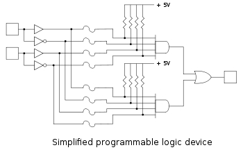
Programmable Logic Devices
(PLD)
As the name suggests, when Programmable
Logic Devices (PLDs) are manufactured, they do not have a
fixed logic configuration. In comparison to an IC with
dedicated logic gates such as ORs, ANDs, etc., they have a
large number of unallocated gates and flip-flops that can be
configured though programming to perform custom logic
functions.
Simple PLDs (SPLDs)
The earliest types of these programmable
devices are now categorised as "Simple PLDs",
and are used for fixed functions and smaller circuits with a
limited number of gates. Types of SPLDs include the
Programmable Array Logic (PAL)
devices that Memotech used for RAM/ROM address decoding in
the MTX computer. (For some additional details on Memotech's
use of PALs, see my
PAL Reader
page.) These devices are one time programmable, programming
was performed by "blowing" interconnecting fuses in the AND
array.
The Generic Array Logic (GAL)
device is another type of SPLD, a development of the PAL
that it is electrically erasable, so could be reprogrammed.
As PALs are all but unavailable today, with suitable
programming, GALs may be used to replace PALs in legacy
products.
|
PLD Internal Structures |
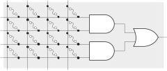
| A typical array structure used in PALs and
GALs.
The example shown is of a blank PAL, prior to
programming, all of the fuses are intact. |
 |
|
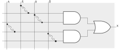
After
programming, the blown fuse links are
permanently open and the array structure now
performs the programmed function, in this case
:-
(A
. B) + (A .
B),
i.e., the XOR function
|
 |
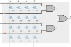
| The same structure illustrated for a GAL.
The "fuses" can be reprogrammed, allowing the
GAL to be reused, this is particularly useful
during development compared with a PAL where a
new device would be required every time that it
was necessary to change the program. |
 |
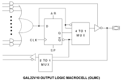
| After the input AND array, PALs and GALs
have output logic that connects to OR gates from
each of the AND arrays. The combined input and
output logic is together referred to as a
macrocell.
A typical example is shown here, for a
Lattice Semiconductor
GAL22V10. |
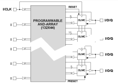
 |
| The Lattice Semiconductor Functional Block
Diagram for the GAL22V10. There are 12
dedicated input pins and 10 pins
that can be configured as either inputs or
outputs, leading to the device name GALxxVyy,
where xx = inputs and yy = outputs, in this
case, GAL22V10 |
 |
Complex PLDs (CPLDs)
|
CPLD Internal Structure |
|
Complex PLDs consist of multiple
Logic Array Blocks (LABs) which
are effectively multiple SPLDs and
interconnections on a single chip.
The LABs are connected via a
Programmable Interconnect Array (PIA)
|
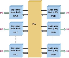 |
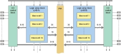
| A portion of an Altera MAX7000 series of
CPLD is shown here and illustrates the typical
structure of of a CPLD. |
 |
| Note : CPLDs
are well suited to applications which mainly
require
combinatorial logic, but typically have a
very limited number of macrocells available
which limits the amount of sequential logic or
register storage that can be used, for such
applications it is more appropriate to use an
FPGA.
The specific structure and
operation of the EPM7128SLC84 to be used in
MTXPlus+ is described in more detail on the
following pages, which includes some further
discussion of macrocells.. |
Field Programmable Gate
Arrays (FPGAs)
Field Programmable Gate Arrays are devices
with even more flexible structures than CPLDs, with much
larger capacity and integral RAM. (As FPGAs will not be used
in MTXPlus+, they are not discussed further here.)
CPLD
Overview <
Previous
Page Goto
Next
Page >
EPM7128S Overview
References :
Digital Fundamentals, 10thEdition, Thomas L. Floyd, Published by
Prentice Hall, ISBN 0138146462 (ISBN13: 9780138146467)
|