|
"MTX Plus+" CPU Board V 2.0
|
CPU Board Specifications -
Version 2 |
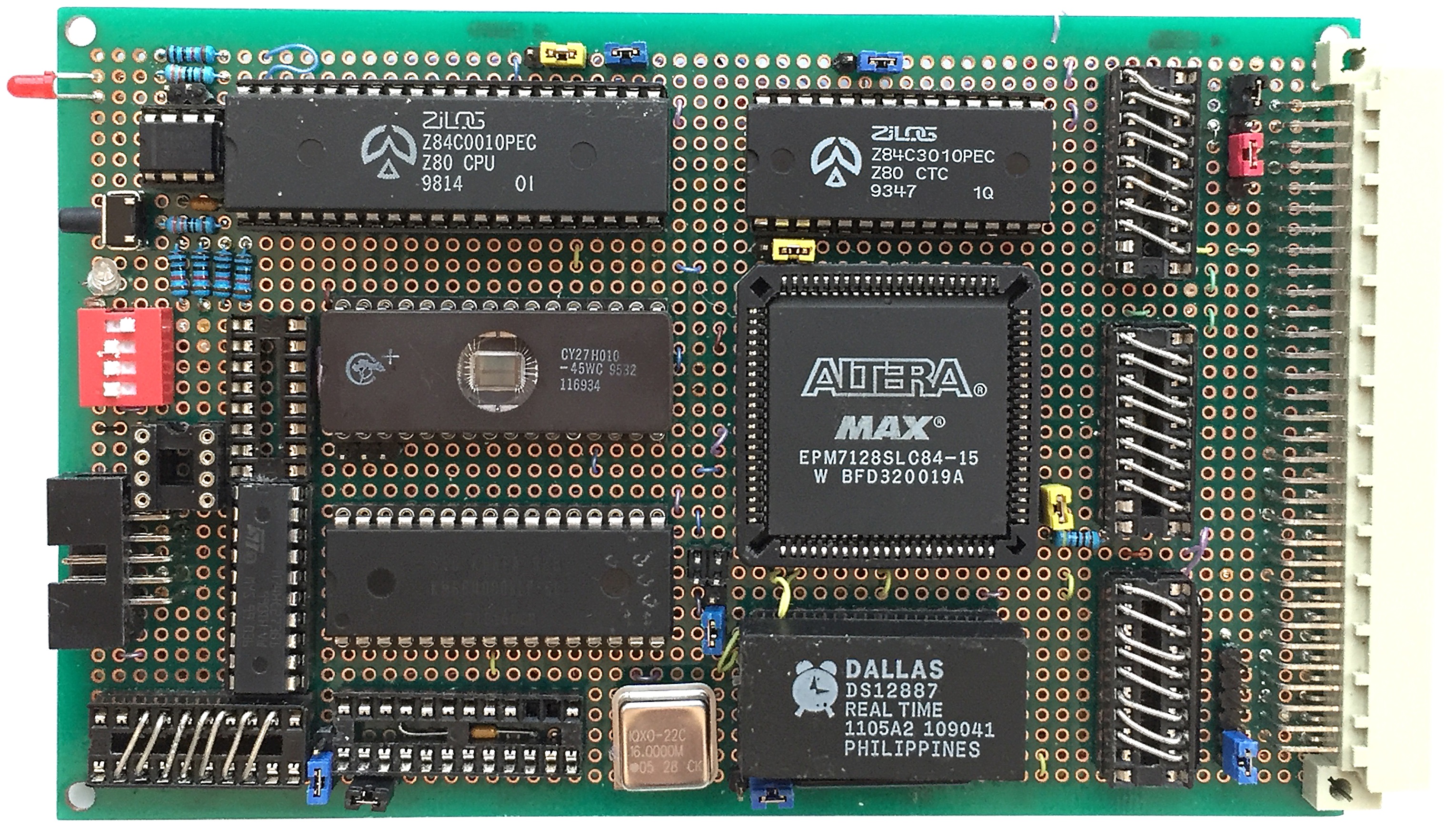
| CPU |
Z80 |
20 MHz DIP40 Package |
| Clock Speed |
16MHz |
With 8MHz, 4MHz and Ck4/13 (for
serial ports) sub-clocks |
| RAM |
512kB |
Static RAM, rather than the
Dynamic RAM (DRAM) used in the MTX
Optional
additional SRAM, making up to 784KB of RAM available |
| (512kB) |
| ROM |
128kB |
For additional details of the ROM
configuration, see the
Memory
page |
| Glue Logic |
|
Altera Max CPLD (EPM7128SLC84) (Or 3
x GAL) |
| CTC |
Z80CTC |
Z80 Counter/Timer for serial clocks
and interrupt processing |
| RTC |
DS12887 |
24 pin encapsulated package |
| Reset |
MAX705 |
DIP8 Package - for uP supervisory
functions (CPU reset) |
Overview
Hardware - Control Bus Signals - Version 2
Board
The backplane distributes a number of control signals to the
rest of the boards in the system, the majority of these are
standard Z80 control bus signals, generated by the CPU, but
there are also a number of other signals generated or used on
the CPU board that are distributed over the backplane.
| Name |
Description |
Source |
Direction |
| PHI |
System
clock signal (frequency set by bit switches 0 to 2)
|
Bit |
0 |
1 |
2 |
Frequency |
|
|
0 |
0 |
0 |
16 MHz (default) |
|
|
0 |
0 |
1 |
8 Mhz |
|
|
0 |
1 |
0 |
4 Mhz |
|
|
0 |
1 |
1 |
2 MHz |
|
|
1 |
0 |
0 |
1 MHz |
|
|
1 |
0 |
1 |
1 kHz |
|
|
1 |
1 |
0 |
8 Hz |
|
|
1 |
1 |
1 |
1 Hz |
|
CPLD |
To Backplane |
| PHI4 |
Additional 4MHz clock signal |
CPLD |
To Backplane |
| PHI8 |
Additional 8MHz clock signal |
CPLD |
To Backplane |
| SER01 |
Clock for serial port 1 |
CTC |
To Backplane |
| SER02 |
Clock for serial port 2 |
CTC |
To Backplane |
| DIAG |
Signal to the Diagnostic board to
latch 7-segment displays based on logic in the CPLD.
By reprogramming the CPLD and switching the position
of jumper J5, simple on board status conditions can
be shown using the on board "DEBUG" LED. |
CPLD |
To Diag.
board |
| /VDPINT |
Interrupt signal from VDP |
VDP |
From Video
board |
Design & Build
Martin and I will be using the same functional design for the
CPU board, but our implementation of the glue logic will be
different, as I described above, I shall be using an Altera
EPM7128S CPLD whereas Martin is going to use a number of GALs on
his board.
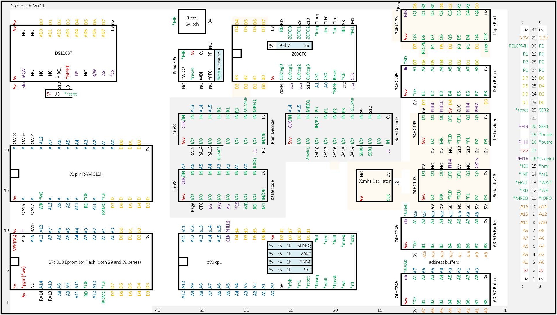
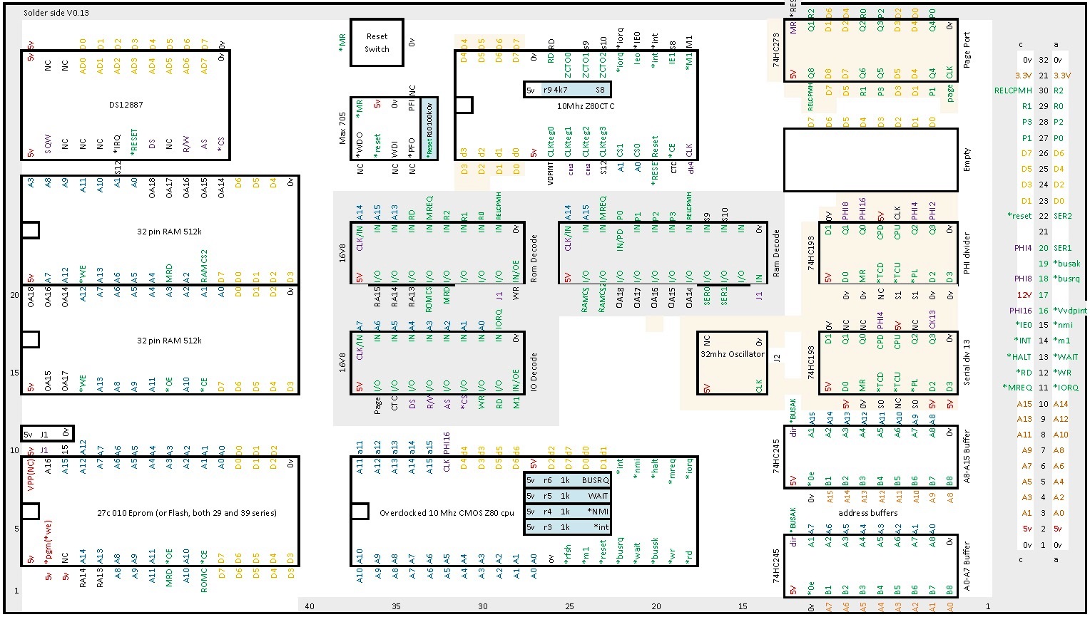
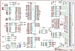
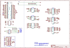
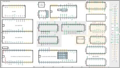
| The draft schematic for my CPU board, including the CPLD. Martin's board is essentially the same, but
the glue logic uses three GALs, a GAL22V10 for RAM
decoding, a GAL16V8 for ROM decoding and a GAL16V8
for I/O decoding. Martin also uses a 74HC273 for the
Page Port outputs and two 74HC193s to divide the
32MHz oscillator frequency to generate the
sub-clocks (16MHz, 8MHz, 4MHz, 2MHz and the serial
port clock, 307KHz). |
 |
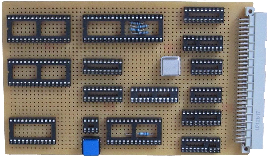
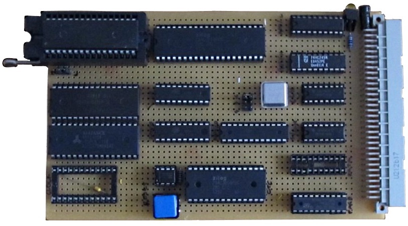
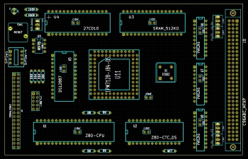
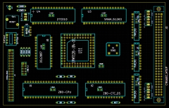
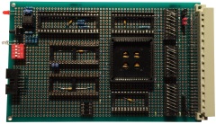
| The component layout for Martin's board (viewed
from the solder side), the GALs are the three chips
in the shaded area in the centre of the board - the
CPLD on my board will be located in the same area. |
 |
| As usual, Martin's construction is a bit ahead
of mine, a couple of photos of his board at various
stages are shown here. |
 |
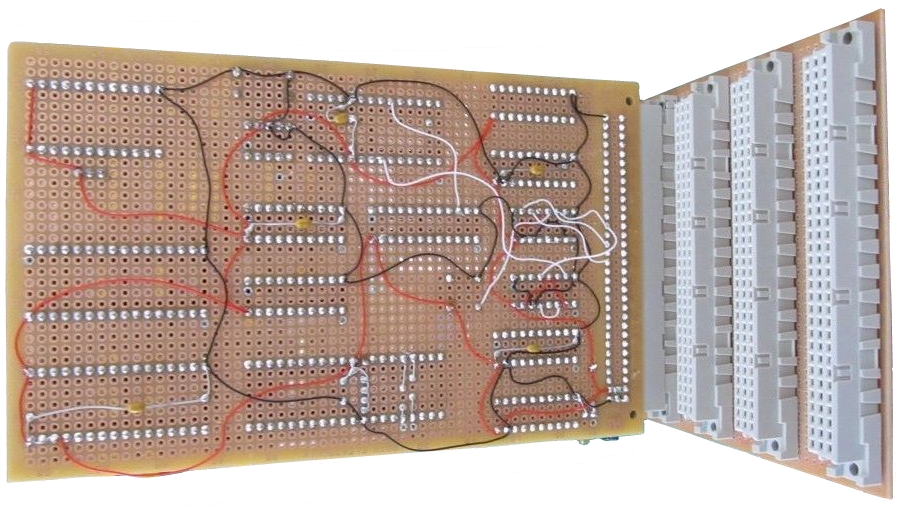
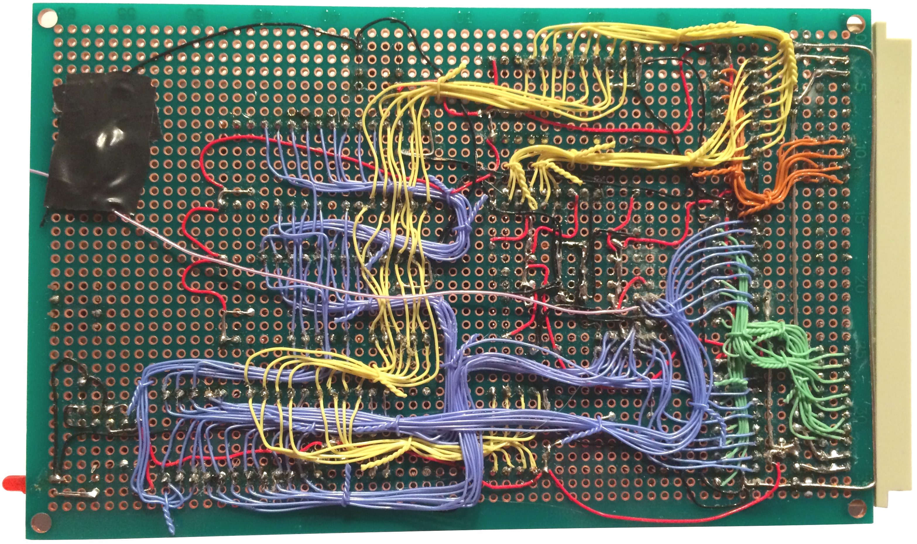
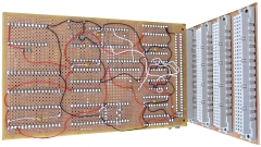
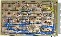
| The solder side of Martin's board, plugged into
his backplane. Just the power and ground
connections have been wired at this point. |
 |
| Version 2.04 of the CPU schematic. Page 1
includes the components common to the CPLD and PLD
designs.
Page 2 shows the components for the two designs
separately |
 |
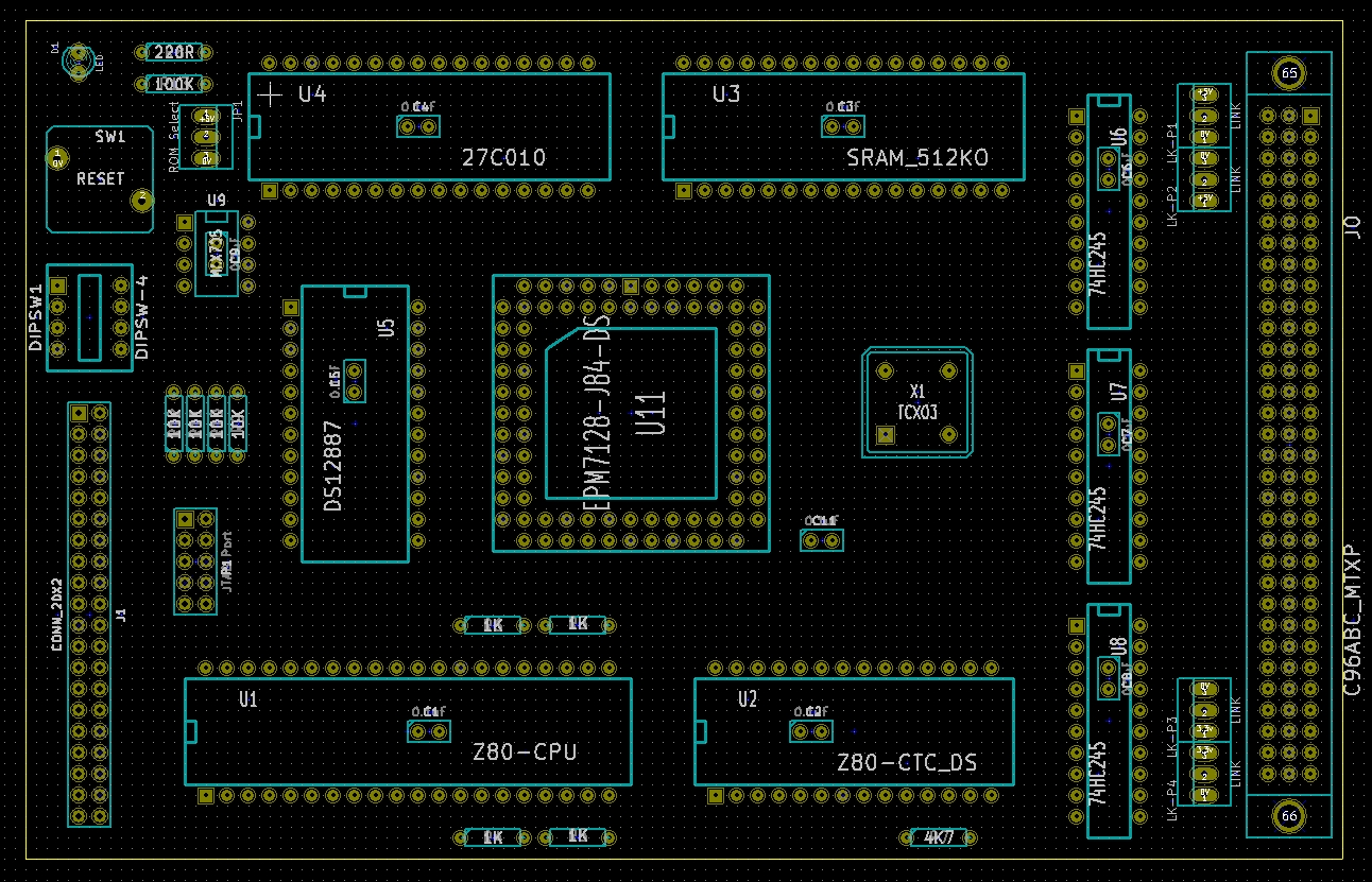
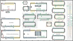
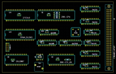
| KiCad PCB layout for the CPLD based design
(Ver.2.02 ds) |
 |
| KiCad PCB layout for the CPLD based design
(Ver.2.02 ma) |
 |
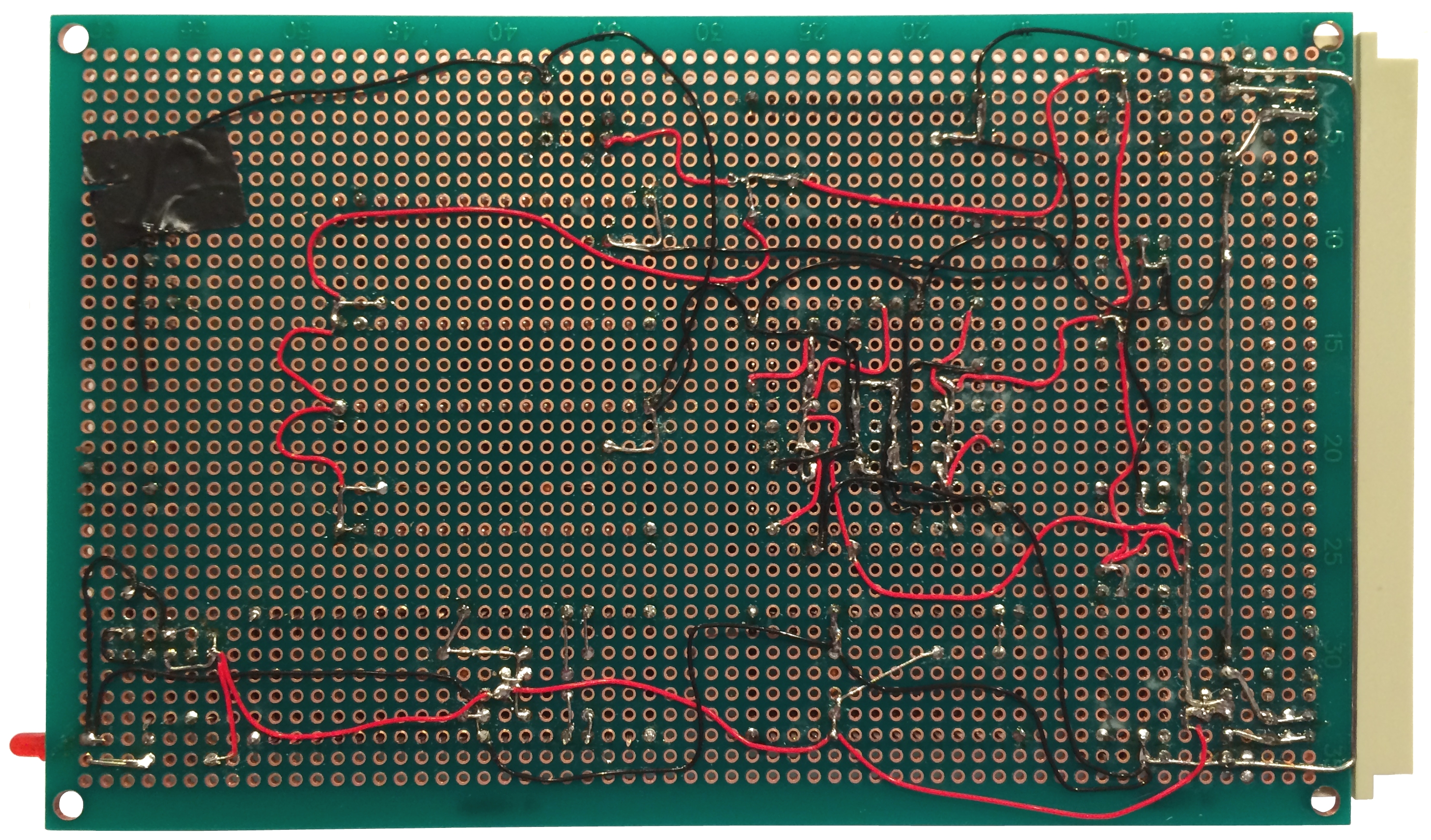
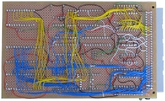
| Another update on the status of Martin's board -
with the address lines wired up to the relevant ICs
(blue) and the memory bus lines connected to the
74HC245 buffer, in preparation for wiring out to the
required IC data connections (yellow). |
 |
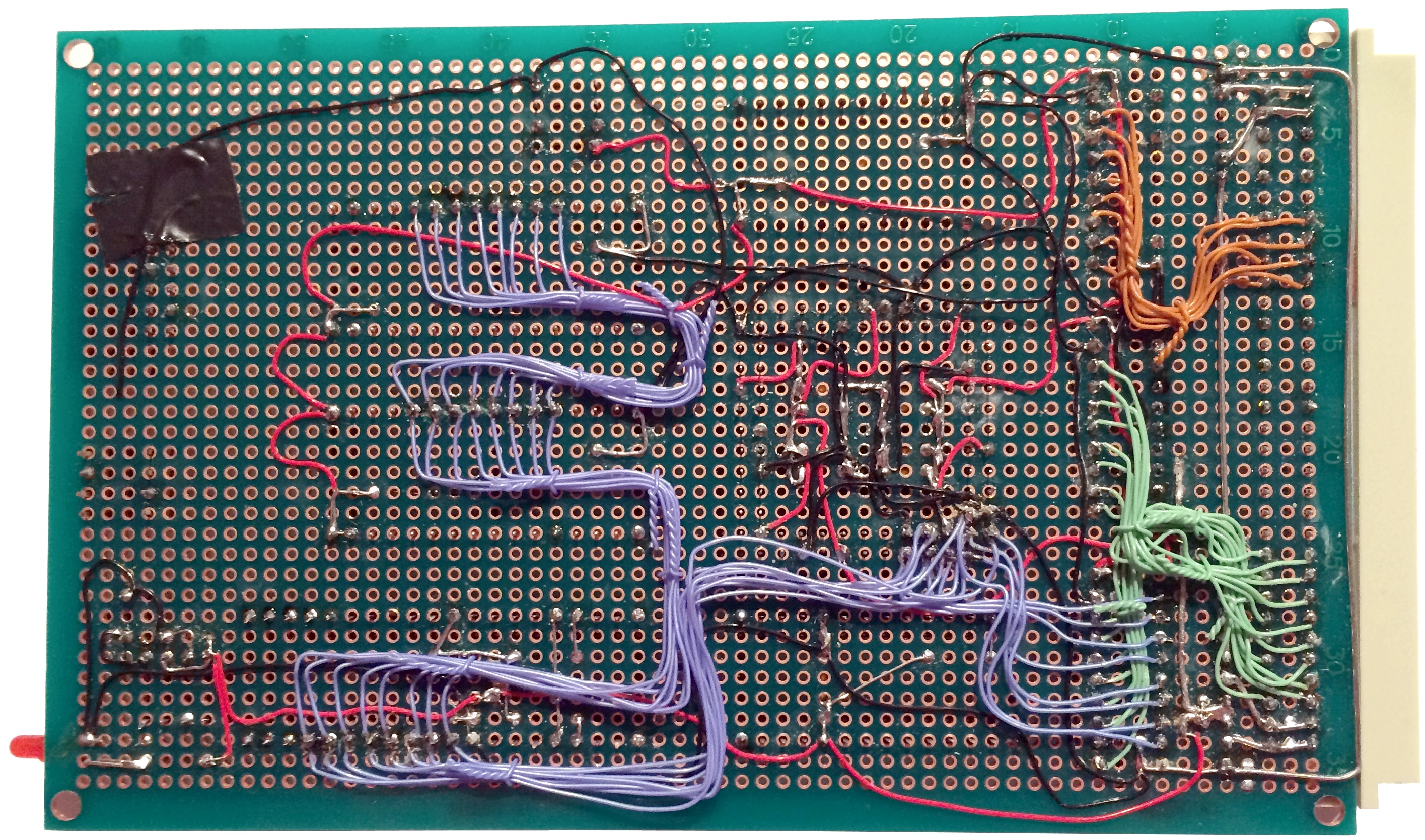
| And now with the data bus completed - "only" the
control signals left to do |
 |
| Some way behind Martin, my CPU board is finally
taking shape . . . .
You may have noticed that the layout is a bit
different to the schematic, I did a little more
"optimisation" when I was test fitting the sockets
which will hopefully make wiring it up a little
easier. |
 |
| Now with the power distribution wiring done on
my board.
As you can see, the wiring below the PLCC socket
is a bit congested, this is due to the 8 pairs of
power and ground connections, along with decoupling
capacitors. The caps are squeezed into the space
between the base of the socket and the top surface
of the board - they are visible in the component
side photo. |
 |
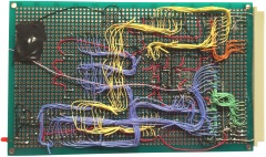
| Some progress on my board, A0 to A15 and D0 to
D7 have been wired from the bus connector to the
buffers and A0 to A7 have been fully wired up, i.e.,
from the buffer to the CPU, ROM, RAM and CPLD. |
 |
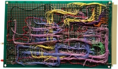
| Now with the rest of the address lines wired
from the buffers to the CPU, ROM and RAM. A13 to A15
are wired to the CPLD where the address decode logic
will generate the OA14 to OA18 and RAMCS signals for
the RAM and the RA13 to RA15 and ROMCS signals for
the ROM. (These are currently not wired.)
I guess that the board is about 40% wired up at
this point. |
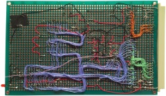 |
| Now with the data bus lines connected to all of
the required components. Like Martin's board
above, "only" the control lines are left to wire,
but that is still quite a few terminations to go.
Most of them are "point-to-point", rather than being
multi-dropped, so it should be relatively quick to
do the final terminations. |
 |
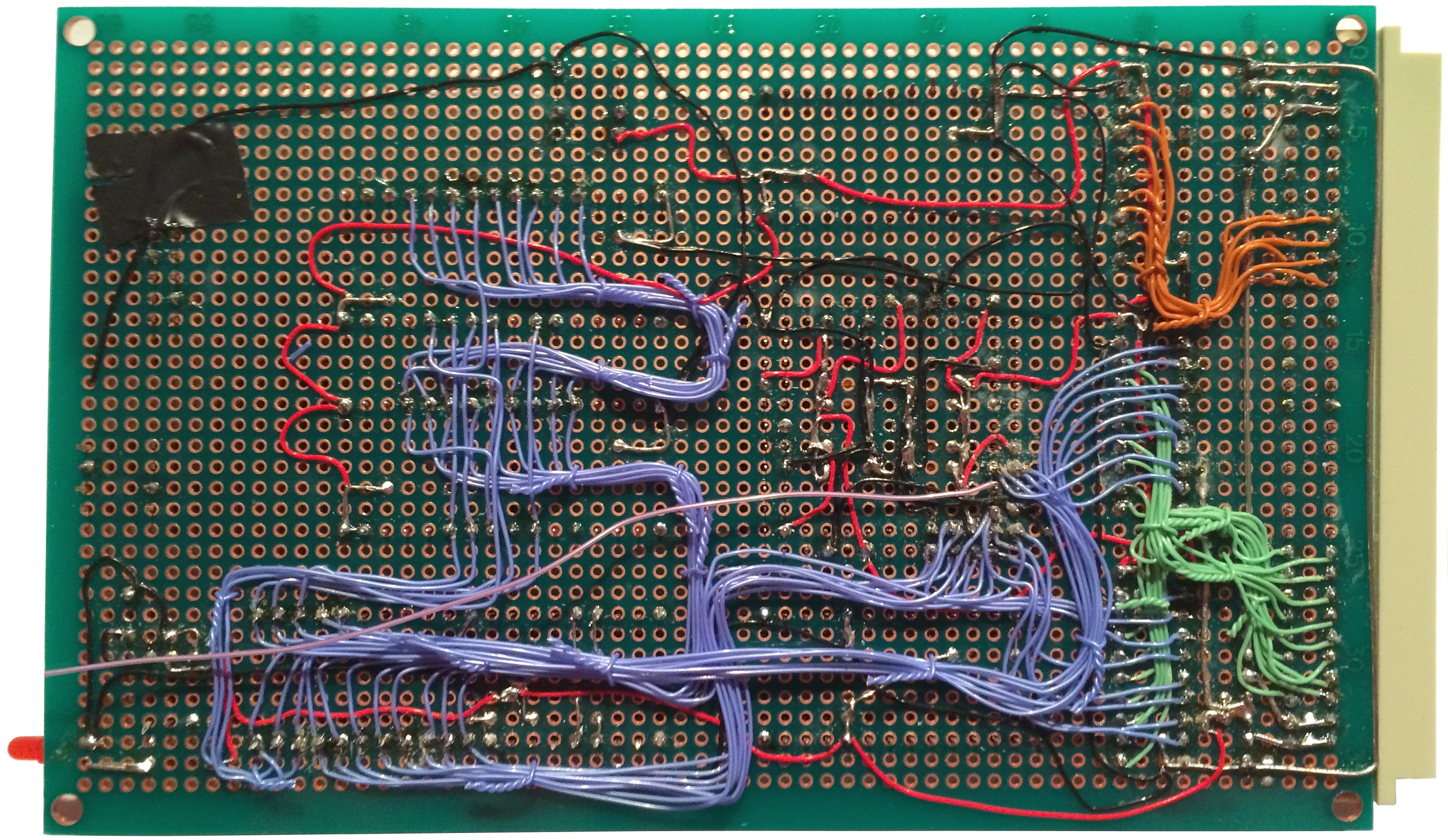
| Another update from Martin . . . .
Almost complete, just the GAL wiring to be
completed |
 |
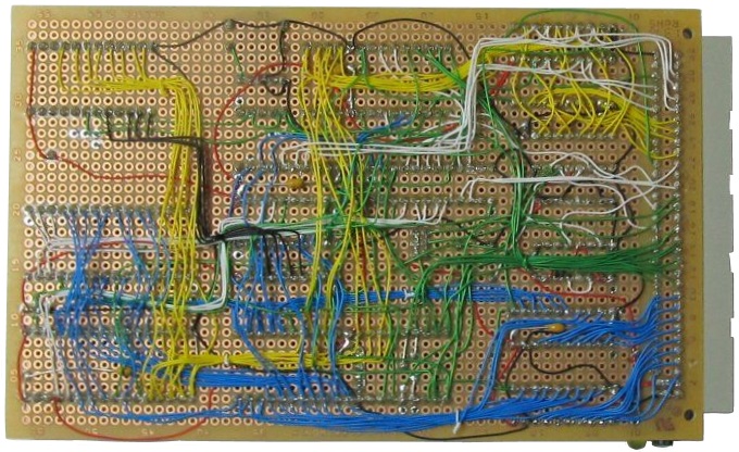
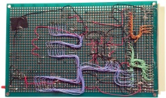
| The wiring side of my completed board, I need to
tidy of some of the longer wire runs, but it's
essentially finished - subject to testing of course. |
 |
| And the component side . . . .
The ROM A16 jumper has now been fitted adjacent
to the ROM socket and an additional jumper installed
at the top left corner of the board to select
whether or not the
RESET signal is applied to the RTC.
(The
RESET pin has no effect on the clock,
calendar, or RAM) |
 |
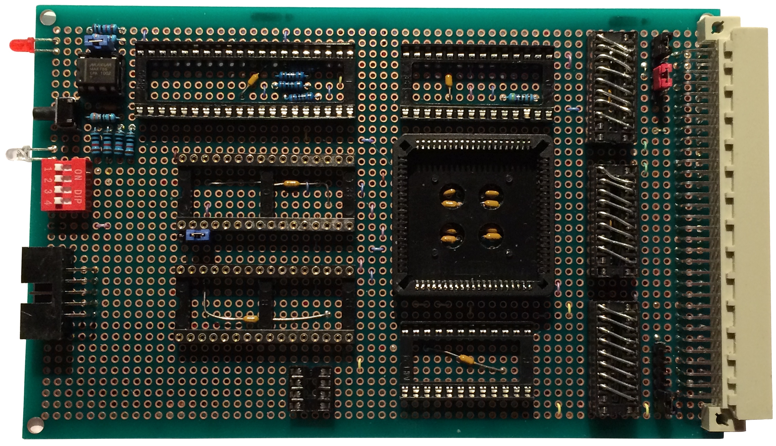
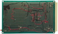
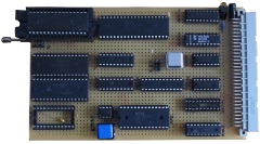
The "final" version of the board, with some
modifications made during development, including a
buffer for the Z80 control lines, a 74HC273 for the
Page Port, a GAL22V10 for Video speed optimisation
and a dedicated 4MHz oscillator for PHI4.
In
this photo, the Address, Data and Control buffers
have been bypassed using shorting links, they were
removed from the final design. |
 |
Testing
Martin and I will be using different testing strategies,
Martin has gone straight to populating the board and programming
the GALs with a minimum configuration to enable 32K of the 512K
SRAM and the standard MTX ROMs in slots 0-2.
Martin's Testing
Martin's first test was to install a copy of his
RAM-less test ROM on the CPU board and run it together with
the Video board and diagnostics board plugged into the bus.
However, no output was generated on the video display, the
symptoms were the same as those seen on an MTX with bad RAM,
i.e., a black display and constant tone from the sound chip. The
status lights on the diagnostic board were also displaying
unpredictable sequences and statuses.
After trying various combinations or ROM, RAM and GAL logic,
Martin found that with the data buffer installed, there was no
output from the video board, but with the buffer linked out, the
display was active.
|
Initial Testing |
| With the GALs programmed to decode a 16K fixed
ROM and 32K of RAM with no memory paging and the
data buffer replaced with jumpers, Martin was able
to boot the CPU from a copy of his test ROM. When
either the 74HCT245 data buffer or the 74HCT273 Page
Port flip-flop was installed, there was no output to
the display, so there appeared to be something amiss
in the data bus. |
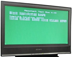 |
| The display shows the
stack test running at RAM location FF00 and the data
read back is incorrect. In a similar test with the
stack test pointing to a location in ROM, the
read-back was correct, suggesting that the problem
may have been with writing data. Using a range of
different addresses and data values for the RAM
stack test, there was no indication of obvious
faults such as stuck or inverted bits. When run
with a clock frequency of 4MHz, the video display
was as shown, when run at 8MHz, the test ran, but
with some display corruption but at 16MHz, the
system "black screened". The display corruption at
8MHz was corrected by inserting some delays in the
VDP output routines to comply with the VDP specs,
but even with delays inserted, the system would not
run at 16MHz.
At this point, Martin thought that the issue with
the system failing to run at high speeds was down to
either the VDP timing still not being correct or
there being an issue with the CPU - perhaps due to
noise or skew or the like. There were strong
indications that it was a CPU issue as the CPU was
actually HALTing when not instructed to. |
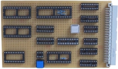
| After trying various things such as installing
additional bypass capacitors and trying another RAM
chip without success, Martin decided to build the
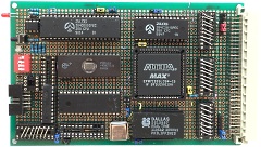
bare minimum CPU board shown here.
In addition to the CPU, the board has ROM, RAM,
clock, a simple R-C reset circuit and a single logic
IC (used to generate a combined logic signal for the
test ROM). |
 |
| For completeness (and as further demonstration
of Martin's wiring skills), the wire side of the
minimal CPU board. |
 |
| Although the screen shot is not very clear and
the colours in the display are not as expected, the
basic CPU board executed the same test ROM code that
failed on the MTXPlus+ CPU board without error. As
with the MTXPlus+ board, the ROM code could be run
at 2, 4 and 8 MHz, but the "black screen" issue was
also present at 16MHz. After a lot of
investigation, mainly by Martin, the symptoms
described had a number of unrelated causes . . . . .
. . |
 |
|
1. Clock Speed
Perhaps
the most interesting issue was that the "20 MHz Z80
CMOS" CPUs that we were using were nothing of the
kind. We found that it was possible to test from
software whether a Z80 was NMOS or CMOS, the test
shown here is running on a CMOS CPU which was able
to run at its labelled speed, whereas the "20 MHz"
versions were NMOS.
More
details of this issue can be found in
this
entry on my
Notes page. |
 |
| 2. Memory Write / Read Errors
Memory write and read-back worked flawlessly on
Martin's minimum complexity test board. Apart from
having a reduced chip count, the main functional
difference between the MTXPlus+ and test CPU boards
was that the test board didn't do any memory address
decoding in PALs.
For testing purposes, Martin modified his
MTXPlus+ CPU board to simplify the memory map,
omitting any memory paging, allocating 16KB of fixed
ROM and 48K of fixed RAM. The ROM decode GAL was
replaced with a single HC32 quad OR, using two of
the gates to drive the ROM chip select
(CS)
signal and the RAM decode GAL logic was reduced to
the bare minimum to enable the 48K of RAM.
SUCCESS
!
- With this simplified memory configuration, the
MTXPlus+ CPU board booted the test ROM and ran the
RAM test routine without errors.
The root cause of the problem was that we had
errors in the PAL (Martin's board) and CPLD (my
board) address decode logic equations. A minimal
memory map was now working and would "just" need
modified to cater for the memory paging required for
the 512K RAM and 128K ROM that we were using.
(You can see the result of the RAM test running
on my board further down this
page) |
|
3.
Video Display Colour Variability
Once the
other issues had been resolved, Martin found that
the variability in the screen colours did not occur on
the MTXPlus+ CPU board. Martin has suggested that it
may have been due to differences in the effect that
the simple RC reset circuit used on the test board
had on start-up of the CPU and VDP, perhaps the VDP
was slower to start and may have missed part of the
register setup code.
As the
MTXPlus+ board, using the MAX705 based reset
circuit, does not exhibit the same behaviour, then
the issue does not really warrant
further investigation.
|
| 4. Data Buffer Problems
See the Design
Development page for details Until the design was modified and changes made to the buffer
wiring and control logic, the work-around was just to run the CPU board with the
data buffer bypassed.
|
|
"Final" Configuration & Testing |
| Memory
Paging |
|
With the core functionality of the
CPU board now working, the remaining tasks were
configuration of the Page Port memory map and I/O
decoding for the RTC in the PALs / CPLD.
This
image shows the output from Martin's test ROM before
memory paging was configured. MTXPlus+ is running with a MTX512 memory
map, i.e., a fixed 16KB of ROM (0-3FFFh) and 48KB of
RAM, including the fixed RAM at 4000-BFFFh and
the "common" block at C000-FFFFh.
With no paging, "Page" faults are reported for the
"missing" RAM. |
 |
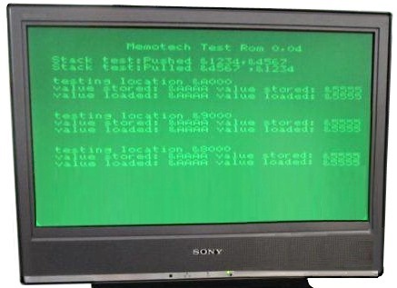
| Once the GAL had been configured for RAM paging, the ROM
was able to find the test the remainder of the RAM
as it was paged into the address
range between 4000 and BFFFh. (The difference in
display colour is due to the ambient lighting when
the photos were taken, the previous photo is closer
to the true screen colour). |
 |
| With the GAL updated to include the
paging code and the MTX ROMs loaded into the on
board ROM, a screen shot of Martin's screen output
which, for obvious reasons, he named "So Close".
Hopefully, you recognise the screen as typical
output from the MTX BASIC ROM. The error is what you might expect if an invalid command had
been entered at the "Ready" prompt. It is likely
that with no keyboard connected, the ROM is still
trying to read the keyboard drive/sense lines and
seeing an invalid key entry. |
 |
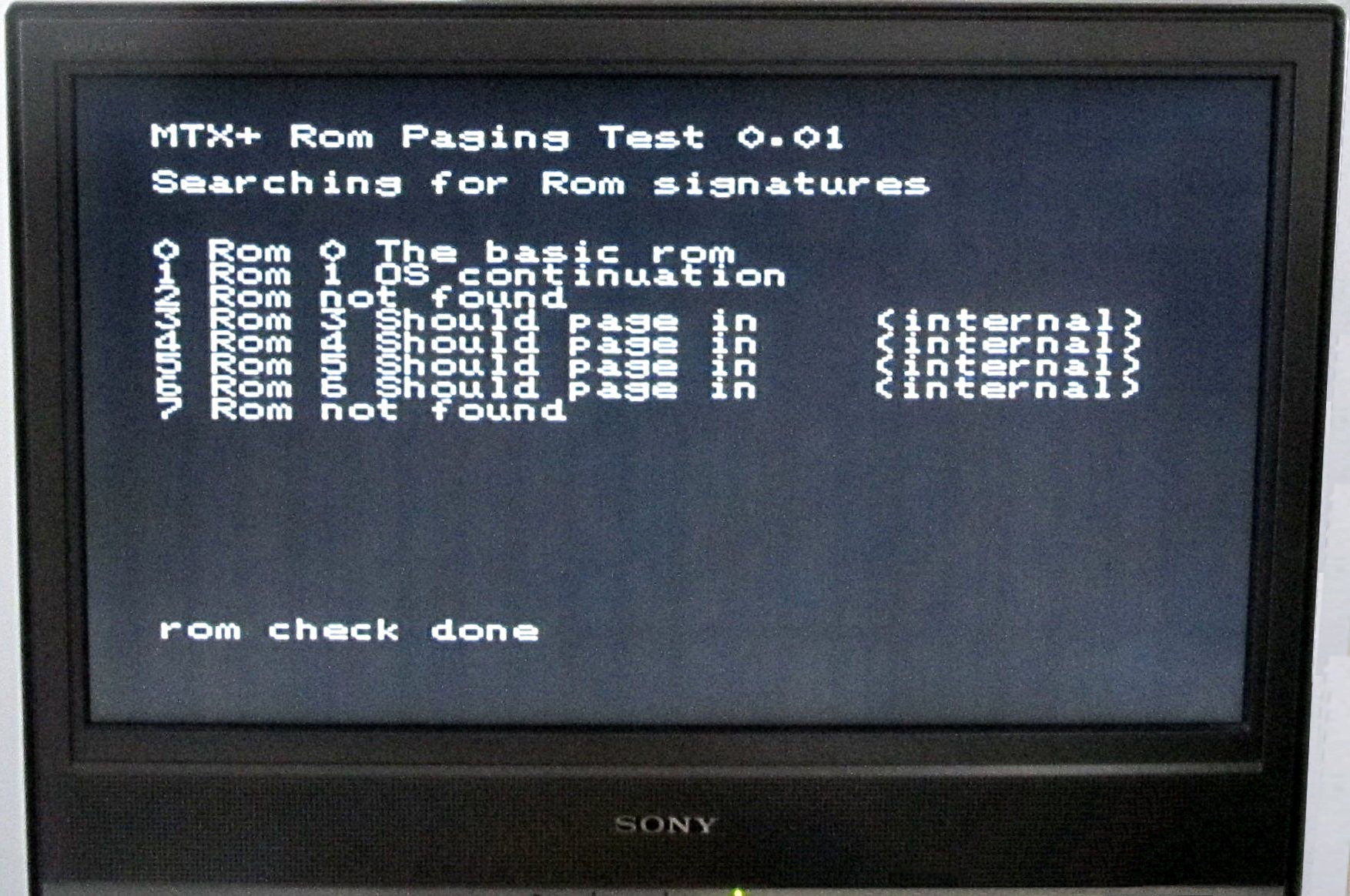
| MTXPlus+ will page ROMs into the
memory as required in the same way that Memotech did
it for the MTX. There is a slight difference in that
copies of the majority of the Memotech ROMs (apart
from ROMs 2 and 7) will be held in the single on
board ROM. The image shows another of Martin's
test programs, this one is checking that the stored
image can be accessed and available for paging. |
 |
| Not content with a "mere" 512KB of
RAM on the board, Martin has allowed a bit of "scope
creep" and made 784KB of RAM available on his board
by squeezing in another 512K RAM chip. |
 |
| You can see the additional RAM chip
squeezed between the original and the RTC ship.
Also note that the ROM is temporarily installed in a
ZIF socket to save wear & tear on the permanent
socket whilst frequent updates to the test ROM were
being made. |
 |
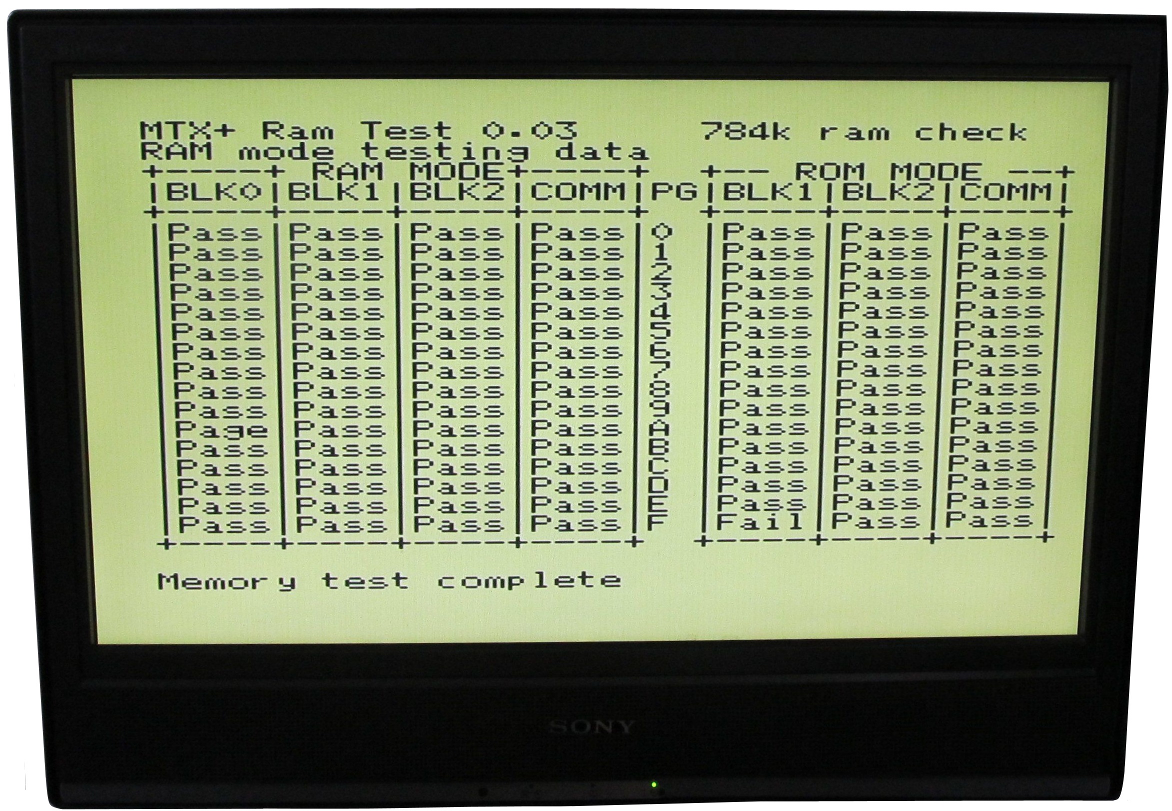
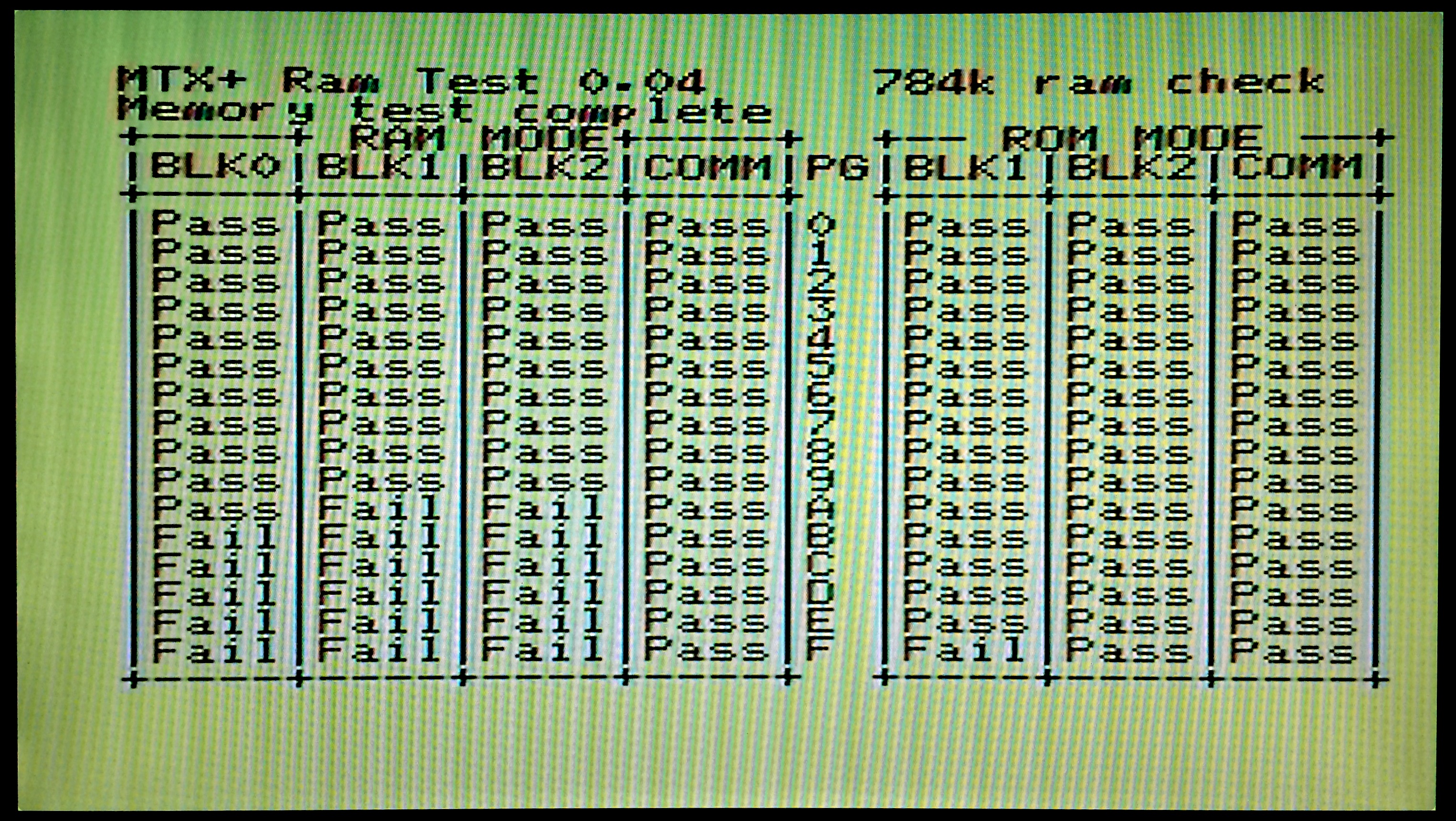
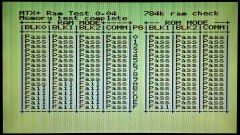
| Martin's test ROM image has been updated
to test the 784KB of RAM. The "Fail" result for
Block 1, Page F in ROM mode is "by design", there’s
nothing to gain from paging in the 2nd chip for just
16k. In addition, the MTX ROM code expects to find a
RAM page failure at some point while its starting
up, as that’s how it identifies the last good page. |
 |
| Real Time
Clock |
| And now with the I/O address for the
RTC being decoded. At this point, the RTC clock
registers are being read, but the clock has not been
reset and displays whatever happened to be in the
registers in the chip. |
 |
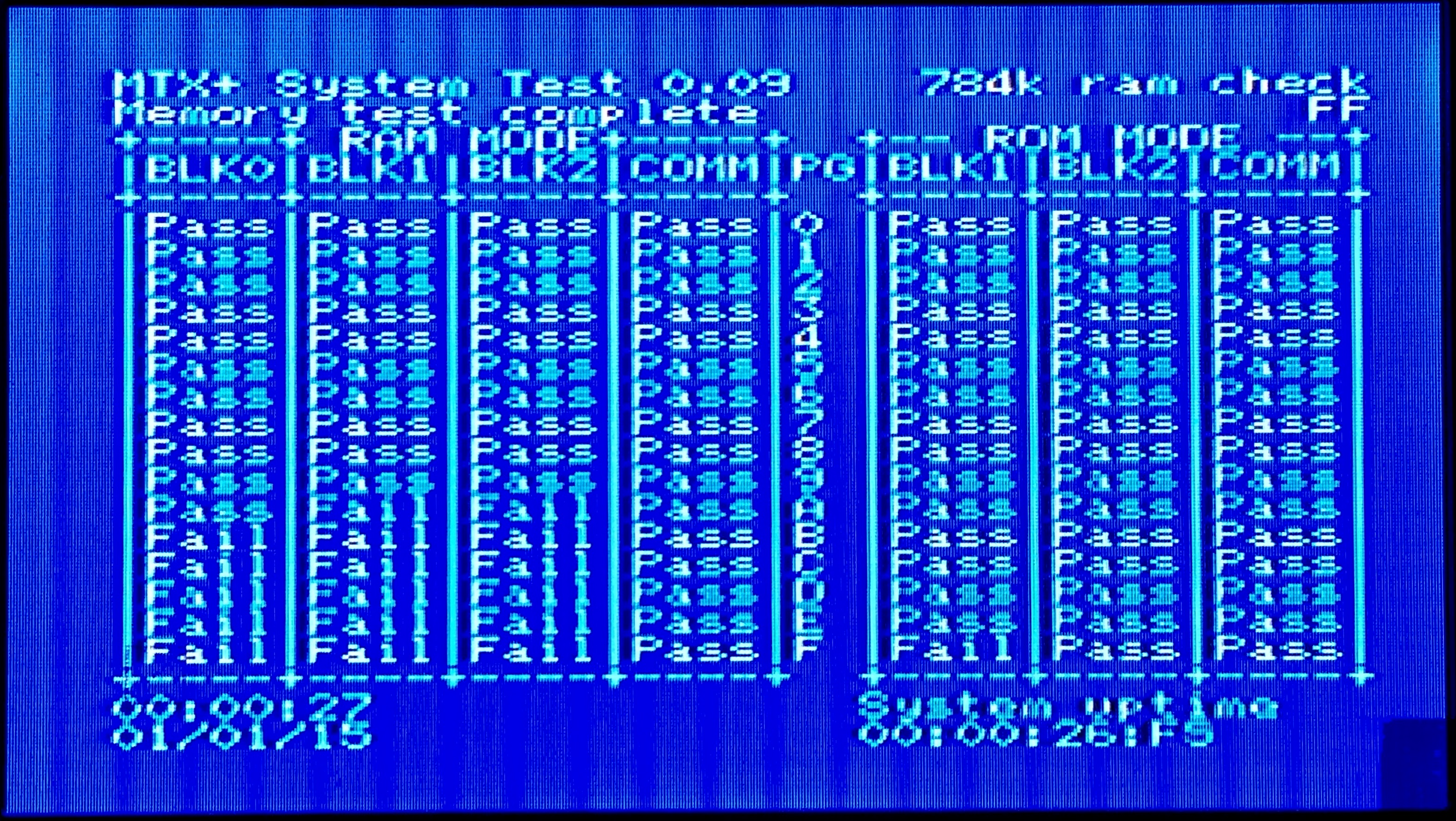
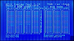
| This photo shows the output from
version 0.09 of the test ROM. At this point, the
clock has been set to 01/01/15 and code has been
added to test the CTC - the "System Up Time" is
being calculated using the CTC. |
 |
My Testing
The pace of my testing was rather more leisurely than Martin's
and my intention was to make use of my MTX to MTXPlus+ bus interface adapter to
test the RAM, ROM and the associated address select logic in
individual stages to make fault finding easier should there be
any problems with the CPU board. As I was finishing off wiring
the board, I thought that a programmable status indicator,
driven by the CPLD, might be useful. Although the CPLD will have
quite a bit of spare logic capacity, there was only 1 spare I/O
pin, as it was likely to remain unused, I wired this out to the
additional LED located above the DIP switch block.
I
had spent a lot of time checking the board against the schematic
with a multi-meter to make sure that the connections went to the
right places. It is easy to check for continuity this way, but,
without testing many adjacent connections, it is not so easy to
pick up short circuits. Nevertheless, I was reasonably confident
that the wiring was OK and the initial test was to connect the
unpopulated CPU board to an MTX and check that the MTX would
operate correctly with the CPU board hanging off the MTX bus.
This did highlight a short circuit after all, there was a short
between +5V and the
M1 signal, which, not surprisingly, gave the
MTX a bit of a problem. That fault was easy to find, and quickly
fixed (the M1
connection to the CPU crossed over a 5V line and a break in the
insulation created the short).
With the CPU board connected to the MTX and the address and
data buffers not fitted, the address and data lines were only
connected as far as the buffer input pins. In this mode, only
the control signals, clock lines and Page Port lines are being
fully exposed to the MTX.
Without the buffer chips being installed (and controlled),
I needed to short out the buffer pins to connect the rest of the
address and data bus wiring to the MTX. As the circuit diagram
shows, the buffer inputs and outputs are conveniently located on
opposite sides of the chip - as you can see from the photo, it
was quite easy to make up shorting links - although the quality
of my efforts improved by the time that I got to the data
buffer. It's not really evident from the photo, but to avoid
damaging the permanent sockets, the links are installed in blank
sockets piggy-backed onto the soldered sockets.
With the links installed, no additional faults came to light
and installing the MAX705 allowed the reset
function to be tested. At this stage, I had a Eurocard sized
external reset button connected to my MTX!
Unfortunately though, I was not able to get an MTX to boot
using RAM installed on the CPU board. I initially suspected a
problem with my RAM decode logic in the CPLD and spent some time
working on this until Martin's RAM issue came to light. At that
stage, I abandoned the idea of trying to test from the MTX and
went straight to testing the CPU board with the MTXPlus+ video
board. [It is now pretty certain that my problems were
associated with my memory decode logic, I may go back an test
MTX access to the CPU board at some point - should I ever get
time.]
|
Initial Testing |
| At this point, the
effort involved in building my diagnostic board
proved its worth. I was not able to generate a
display on the monitor, even using a copy of
Martin's test ROM and no RAM installed or
configured. Although I had tested the board with a
meter a number of times, I was unable to find the
problem.
With the test ROM installed and the CPU clock set
to 2Hz, I was able to video the status display as
the program executed and upload the
video to
Facebook to see if
Martin could see anything untoward. Martin was able
to confirm that the program appeared to have loaded
and was stepping through correctly, but spotted that
there was an error in the values seen for A0. Sure
enough, I found that the daisy chained A0 line had become
detached at the ROM pin - so much for my testing!
|
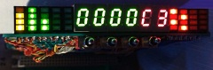
| When the Z80 starts up, it executes its first
instruction from memory address 0 - the image shows
the display on the diagnostic board with the CPU in
single step mode and having loaded the instruction
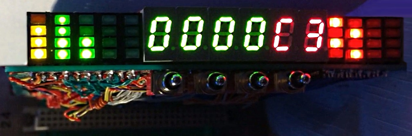
at address 0 - "C3" is the Z80 JP
instruction, and causes the program to jump to the
location stored at the next memory address (in this
case, "7C"). |
 |
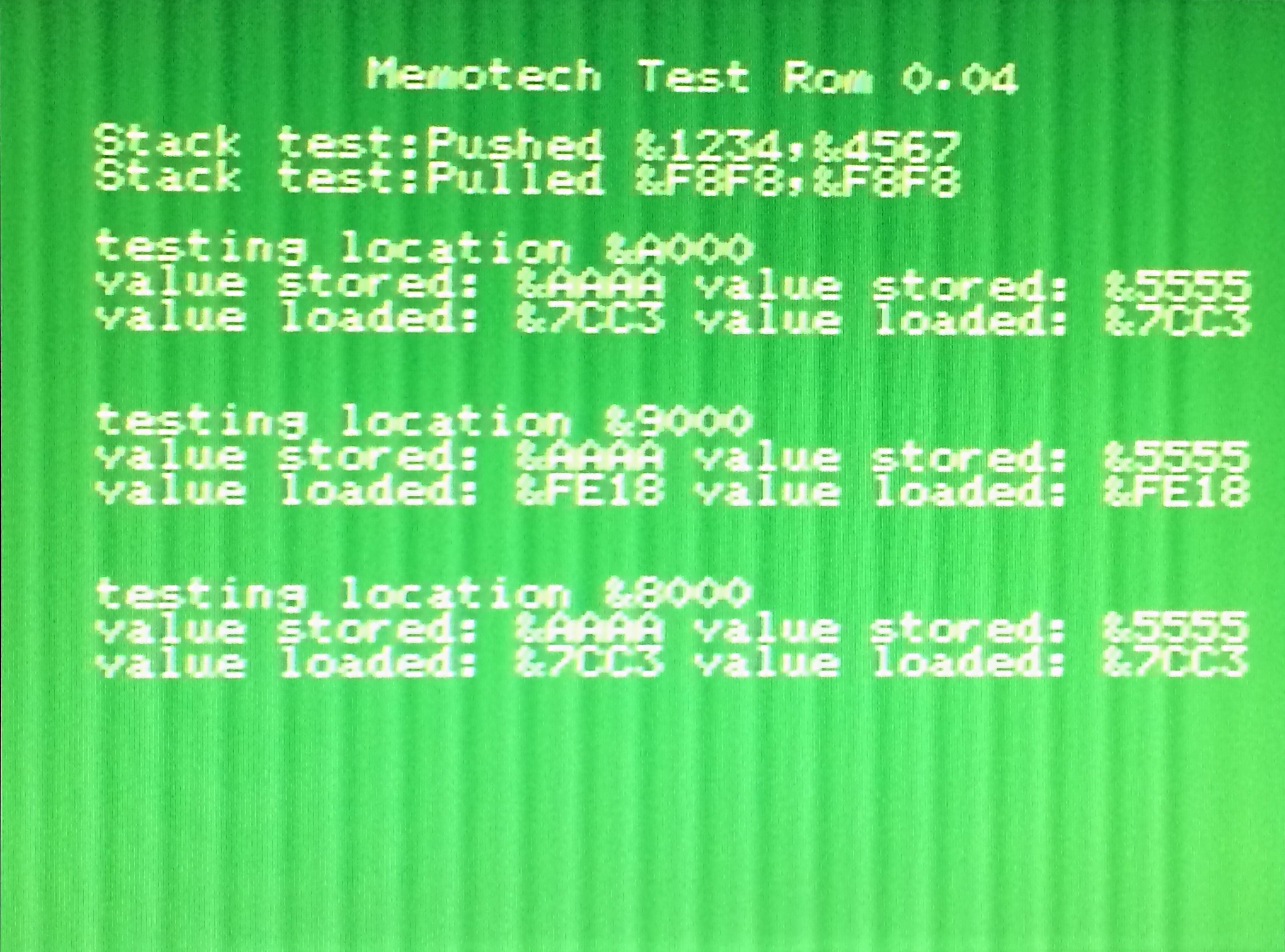
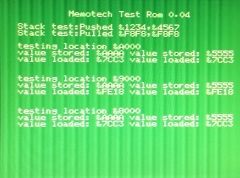
| Having fixed the A0 problem, I was able to see
the output from Martin's test ROM running on my CPU
board.
As shown here, the memory write & read-back tests
failed, confirming that the problem was common to
both designs was and was more likely to be due to a
design/configuration problem, rather than
constructions errors. |
 |
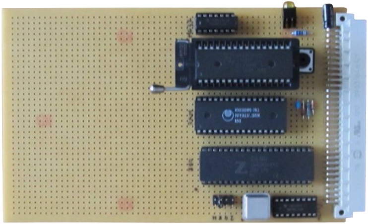
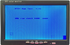
| To save a bit of space while I had a lot of equipment on my test
bench (or, dining room table, as my wife calls it), I splashed out £16 on a new 7" TFT monitor
off ebay, the output is not brilliant, but for
testing purposes it does the job well enough. The
output of the RAM test running on my CPU board,
using NTSC
composite video output to my cheap monitor (still
with the protective film on the screen which isn't
helping the sharpness of the picture). |
 |
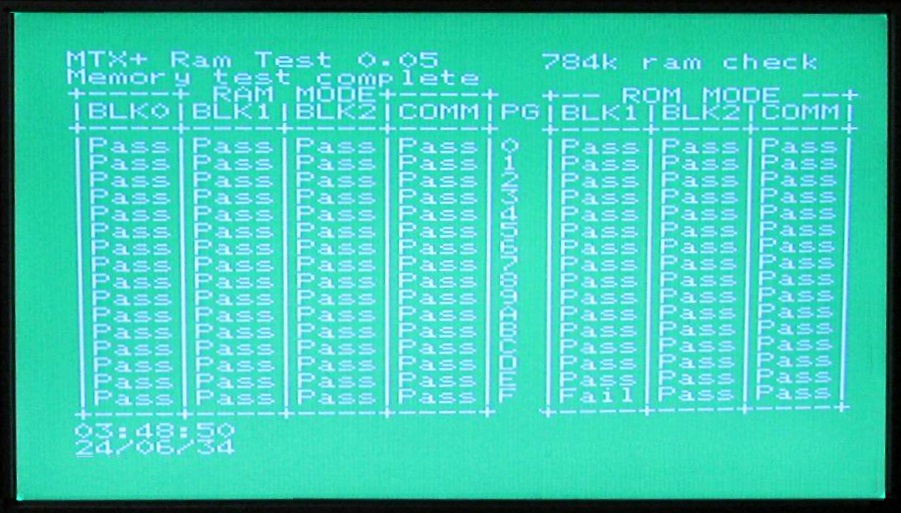
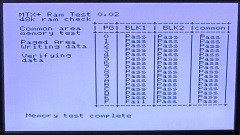
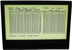
| Martin's 784KB RAM test running on my MTXPlus+,
showing "fail" for the "missing" memory that would
be in the second 512K SRAM. It appears that I may
have the MTXPlus+ equivalent of the MTX500 !
- functionally equivalent to the other
model, but with less memory |
 |
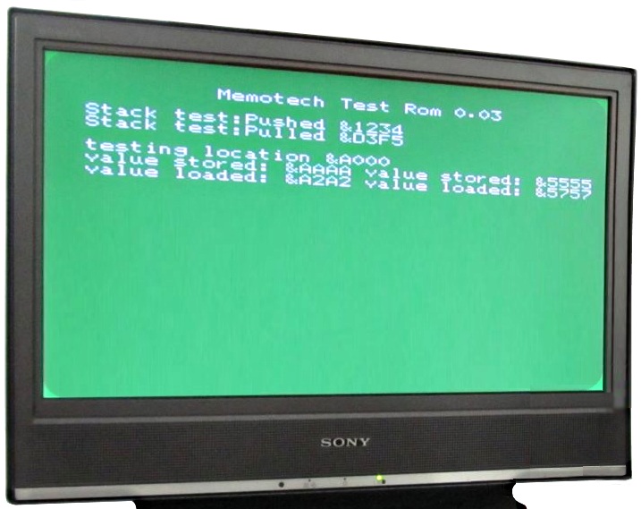
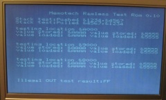
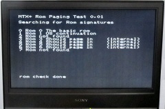
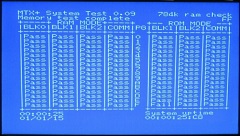
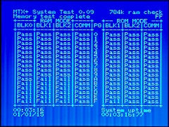
| Version 0.09 of the test ROM running on my
system with output to my cheap 7" monitor.
The image is not too pretty, but all tested
systems, RAM, ROM, RTC and CTC are working as they
should. |
 |
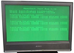
| The same test program with the output to a LCD
TV, using the composite video input and sending a
NTSC signal, screen format set to 4:3 which is
more consistent with MTX and MSX machines using the
same type of VDP. |
 |
|
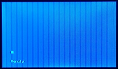
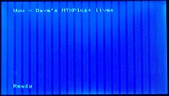
TA DA
!
With the
MTXPlus+
"megaROM" programmed with the standard MTX ROM
images, the usual MTX BASIC "Ready"
prompt was displayed, even before the
I/O board
was connected.
My CPU
board has pull-ups on the data bus that appear to
stop the bad data generating the BASIC error that
Martin had (above). |
 |
|
With the
modified GAL and keyboard
ICs installed, and an original MTX computer keyboard
connected, here you can see the first simple BASIC
program running on my MTXPlus+ The system can
"see" all 512KB of RAM,
PRINT PEEK(64122) returns the expected
"15" for the number of 32KB RAM pages. |
 |
Status Summary
At this point, the CPU board has pretty much been proven to
meet original design intent for MTX compatibility - at
least, when running at 4MHz like the original. However, as
things progressed during the build, a number of changes were
made to correct a couple of weaknesses in my design. Added
to this was some degree of "scope creep" that led to other
modifications and enhancements. These "design
developments" were originally documented on this page, but
the number and magnitude of the changes probably justifies
their description on a separate page that I've called, oddly
enough, Design Development.
The main items are now just bulleted below, for details of
the changes, click on the links to open the new page.
Design Development
|