|
"MTX Plus+" CPU Board V 3.0
|
CPU Board Specifications -
Version 3 |
| CPU |
Z8S180 |
20 MHz PLCC-68 Package |
| Clock Speed |
16MHz |
With 4MHz (for PSG) and Ck4/13 (for
serial ports) sub-clocks |
| RAM |
512kB |
Static RAM, rather than the
Dynamic RAM (DRAM) used in the MTX
Optional
additional SRAM, making up to 784KB of RAM available |
| (512kB) |
| ROM |
128kB |
For additional details of the ROM
configuration, see the
Memory
page |
| Glue Logic |
|
Altera Max CPLD (EPM7128SLC84) (Or 3
x GAL) |
| CTC |
Z80CTC |
Z80 Counter/Timer for serial clocks
and interrupt processing |
| RTC |
DS12887 |
24 pin encapsulated package |
| Reset |
MAX705 |
DIP8 Package - for uP supervisory
functions (CPU reset) |
Overview
My original design for the CPU
board was based on the use of discrete logic chips, like the
original MTX. The design was more or less finalised when I
decided to use a
CPLD in the design to reduce the congestion on the somewhat
cluttered circuit board and to make it easier to modify the
glue logic
should any changes be necessary. This led to the development of
the Version 2 board, you can read about its design, construction
and testing on the Version 2 CPU board page.
Along with the Zilog Z80 CPUs that Lez had given Martin and
I, he had also sent a number of enhanced Z80 CPUs, including the Zilog Z8S180. Martin used one of the Z8S180s to build another
CPU board for MTXPlus+, so I thought that I had better do the
same. As with the Version 2 board, I used an EPM7128SLC84 CPLD
for the glue logic and Martin stuck with GALs.
Based on the results of testing the Version 2 board, I made a
number of changes to the design for the Version 3 board :
- The buffers on the Address, Control and Data lines were
deleted. As MTXPlus+ is mainly based on CMOS technology, the
number of fan-outs was not an issue, so the buffers were an
unnecessary complication that could have an adverse impact
on the potential speed of the system.
- Since no peripheral devices needed it, the fixed 8MHz
clock signal on the bus was removed, freeing up the
backplane line and CPLD output for other purposes.
- The number of system clock divider options was reduced
- Added Q1 to supply power to the diagnostic LED (reducing
the current draw from the CPLD output)
Development and testing of the Version 2 board had shown that
my placement of the I/O in the CPLD was not ideal and required
more LAB resources than was necessary. For example, I had
assumed that assigning all 8 bits of the data bus to the same
LAB would be an efficient use of CPLD resources, as it turned
out, it was actually more efficient to distribute the data bits
between the 8 LABs.
For the Version 3 board, as I had a working version of the
basic CPLD code for the chip select and memory address logic, I
was able to allow the Quartus fitter more freedom to place the
I/O in the most efficient manner, rather than constraining it by
manually placing the I/O when I developed the Version 2 board.
One of the enhancements in the Z8S180 CPU is its ability to
clock its internals and external devices at frequencies of half,
equal to, or double the input clock frequency. The clock
doubling feature only operates effectively with source clock
frequencies of 10-16MHz, meaning that if it is used with MTXPlus+,
the CPLD source oscillator should be no greater than 32MHz,
resulting in an input frequency to the CPU of 16MHz at the
fastest CPU board DIP switch setting.
Whilst this would allow a theoretical clock speed of 32MHz,
this is unlikely to be a realistic target for MTXPlus+,
therefore, the Version 3 CPU board will initially use a 24MHz
oscillator, giving a "stretch" target system clock speed of
24MHz with clock doubling enabled, although 20Mhz is likely to
be the best achievable with my prototype board.
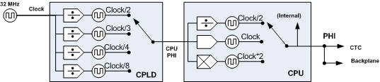
Hardware - Control Bus Signals
The backplane distributes a number of control signals to the
rest of the boards in the system, the majority of these are
standard Z80 control bus signals, generated by the CPU, but
there are also a number of other signals generated or used on
the CPU board that are distributed over the backplane.
| Name |
Description |
Source |
Direction |
| Clock |
Clock source for the CPLD |
X1 |
To CPLD |
| PHI4 |
4MHz clock signal from dedicated
oscillator |
X2 |
To Backplane |
| PHI_CPU |
CPU
clock source signal, assuming 24MHz CPLD source
oscillator with the selected frequency set by bit
switches 0 to 1.
|
Bit |
0 |
1 |
Divider |
Frequency |
|
|
0 |
0 |
2 |
12 MHz (default) |
|
|
0 |
1 |
3 |
8 Mhz |
|
|
1 |
0 |
4 |
6 Mhz |
|
|
1 |
1 |
n/a |
SQW from RTC |
|
CPLD |
To CPU |
| PHI |
CPU Generated clock signal
|
Scaler |
Frequency |
|
0.5 |
6 MHz |
|
1 |
12 Mhz (default) |
|
2 |
24 Mhz |
|
CPU |
CTC & Backplane |
| SER01 |
Base Clock for serial port 1
(307.692 kHz) |
CTC |
To Backplane |
| SER02 |
Base Clock for serial port 2
(307.692 kHz) |
CTC |
To Backplane |
| DIAG |
Signal to the Diagnostic board to
latch 7-segment displays based on logic in the CPLD.
By reprogramming the CPLD and switching the position
of jumper J5, simple on board status conditions can
be shown using the on board "DEBUG" LED. |
CPLD |
To Diag.
board |
| /VDPINT |
Interrupt signal from VDP |
VDP |
From Video
board |
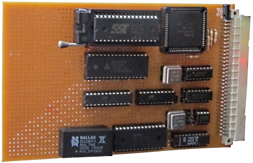
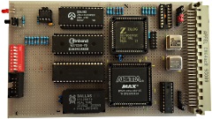
Design & Build
| |
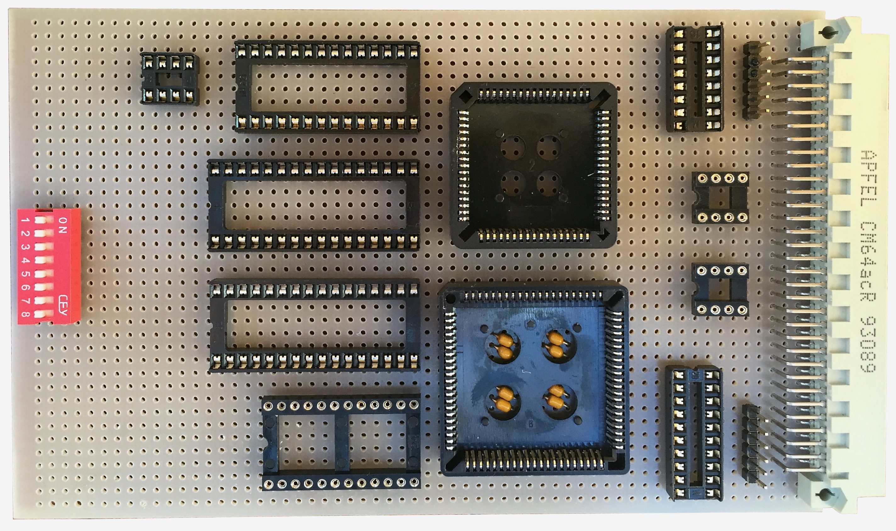
|
Sockets for the main
components positioned, the smaller PLCC (68 way)
socket is for the Z8S180 and the larger (84 way) one
is for the CPLD.
I wasn't able to source more
of the good quality, double sided, prototyping
boards that I had been using, this single sided
board is one of Maplin's and is of much lower
quality than my previous supply. |
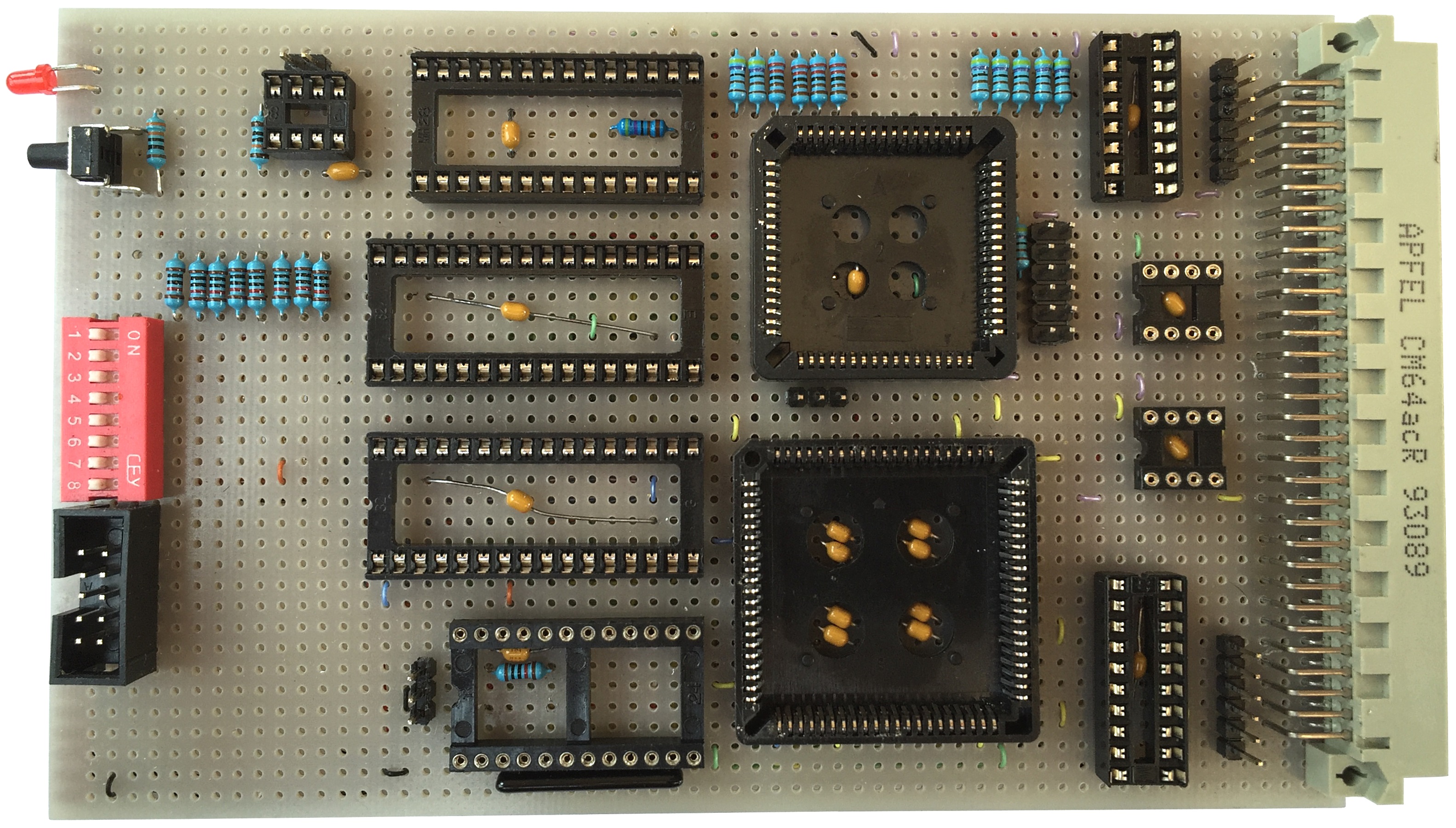
 |
The completed board prior
to testing.
The shrouded 10-way header socket
next to the DIP switches is the JTAG connector. The
12-way header next to the 68-way PLCC socket is
connected to the Z8S180 serial lines. These will not
be used initially, but were wired to the header now,
rather than trying to add additional connections to
the PLCC socket later should they ever be used. |
 |
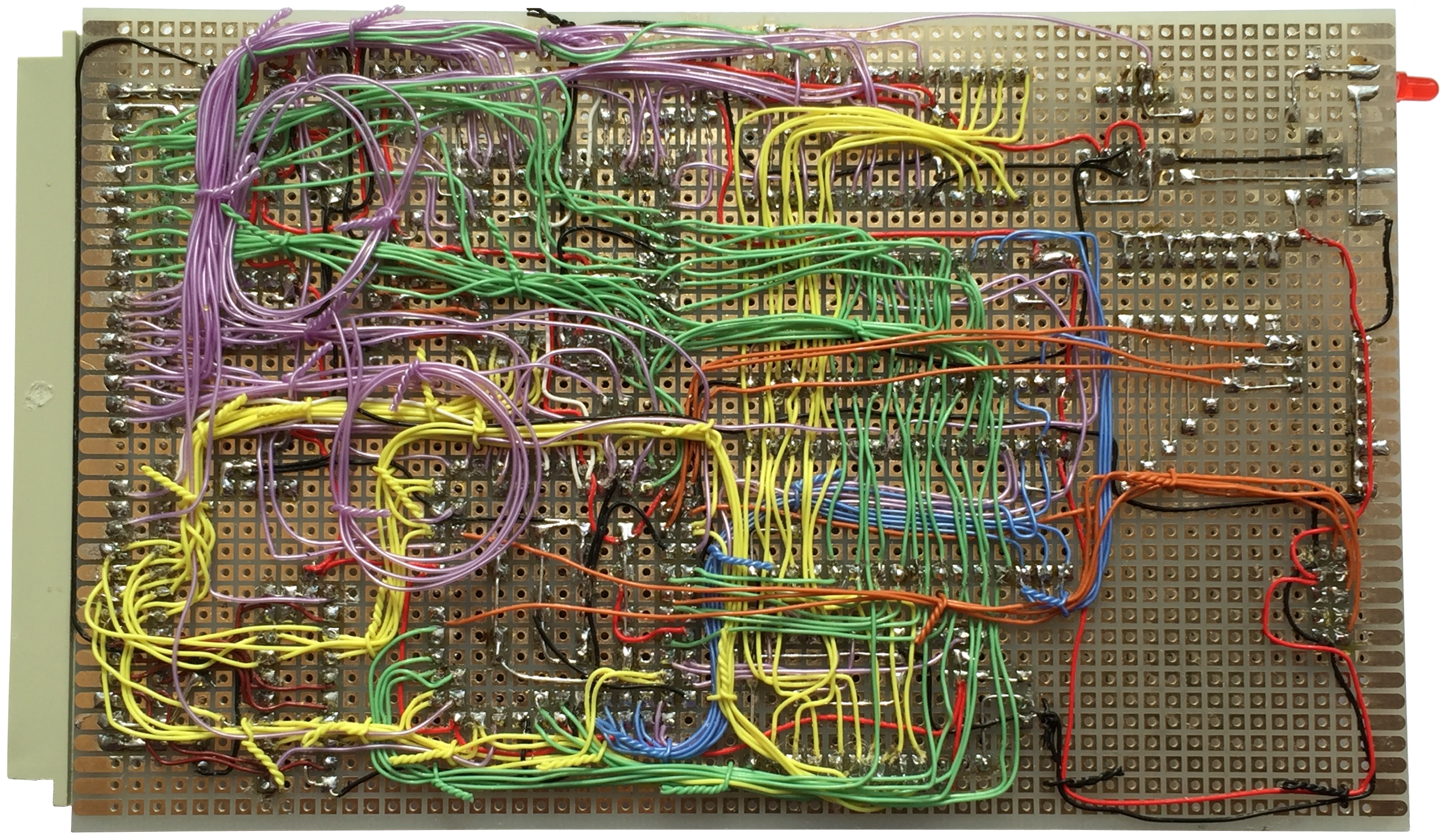
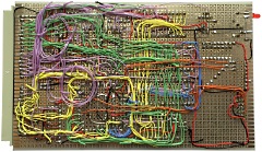
Wire side of the completed
board
Initial testing of the board was done
with a DVM to verify the connections were as per the
schematic, then the CPLD was installed and the ISP
JTAG connector used to load the modified program to
the CPLD. |
 |
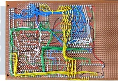
For comparison, the wire
side of Martin's Z180 board.
As usual,
looking far neater than mine! - In my defense, I
would argue that mine is much more complicated
though :-) |
 |
Rather than going straight
to Martin's latest Z180 version of the MTXPlus+ ROM,
I wanted to test the functionality of the board in
discrete steps.
Here you can see the output from a
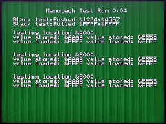
very early MTXPlus+ test ROM, it does not access RAM
and only needs the CPU, CPLD and ROM installed. As
the Z180 uses RAM for its stack, the read-back
fails, but the test does prove that the CPU is
working, it can access the ROM and can drive the
video board (in MTX mode using I/O ports 01 & 02) -
a great start! |
 |
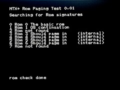
| This test ROM verified that
the MTXPlus+ component ROMs could be read and were
available to be paged in by the MTXPlus+ system. |
 |
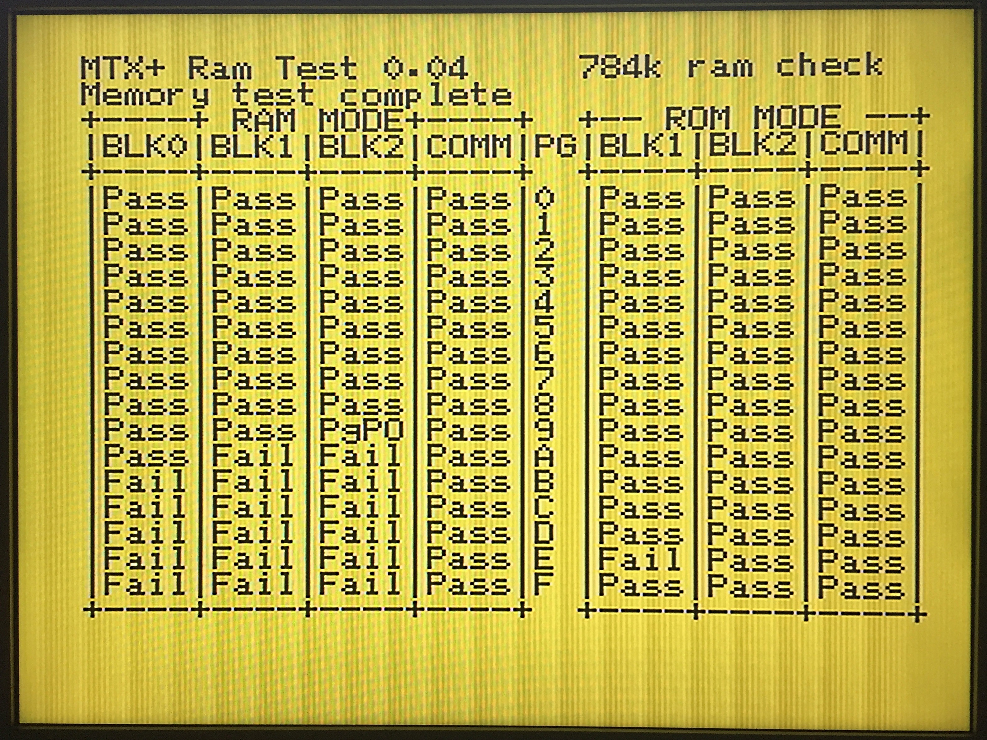
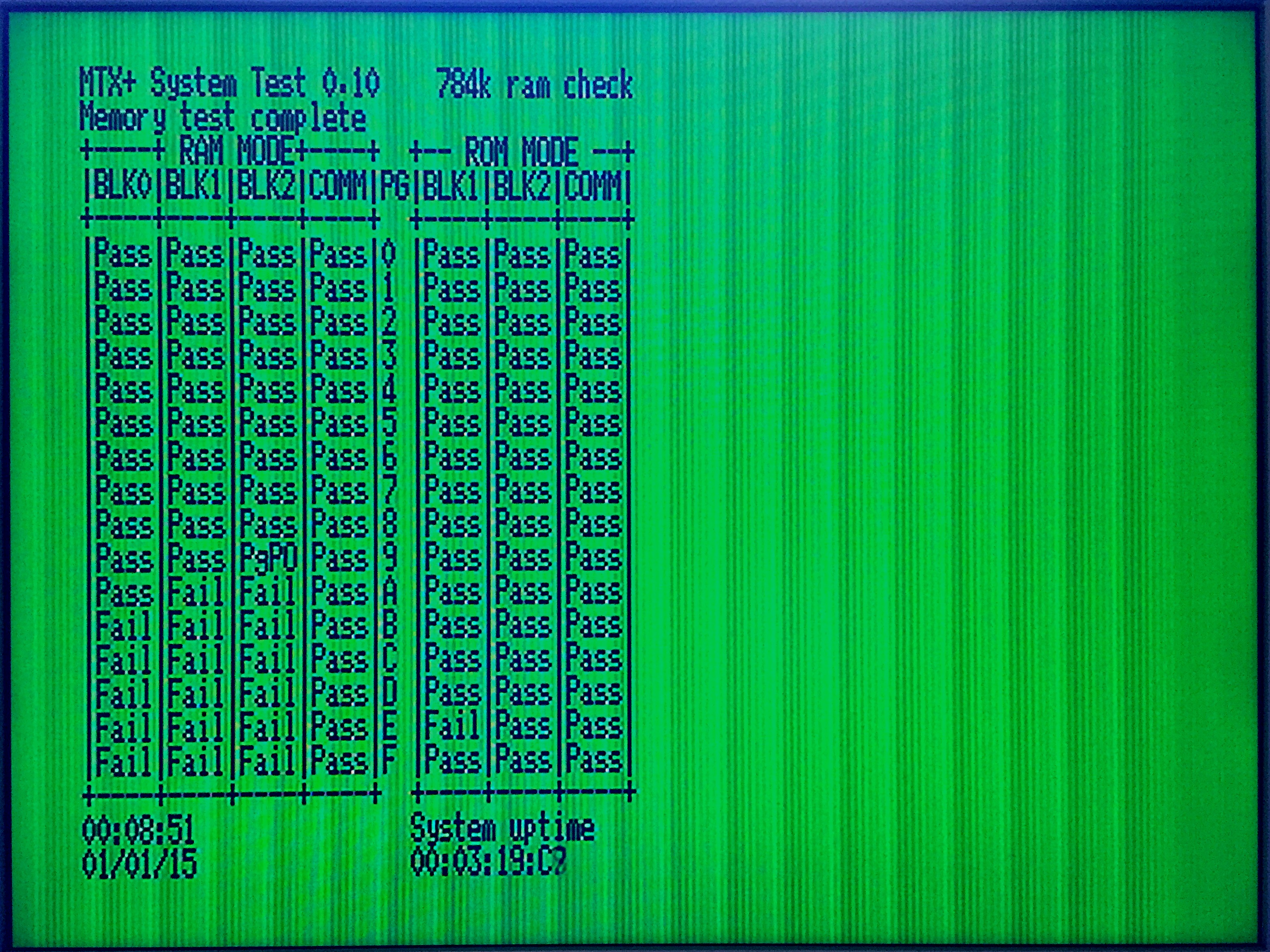
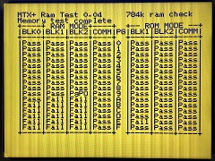
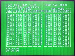
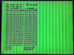
This test ROM checks the
installed RAM and verifies that the extended memory
can be paged into the address range between 4000h
and BFFFh.
The ROM was written to test up to
784kB of RAM - the maximum available on Martin's Z80
CPU board with 2 x 512kB of RAM installed. With
"only" 512k on my Z8S180 board, the failures in the
highest slots are to be expected but the test proves
that the rest of RAM is available and working. |
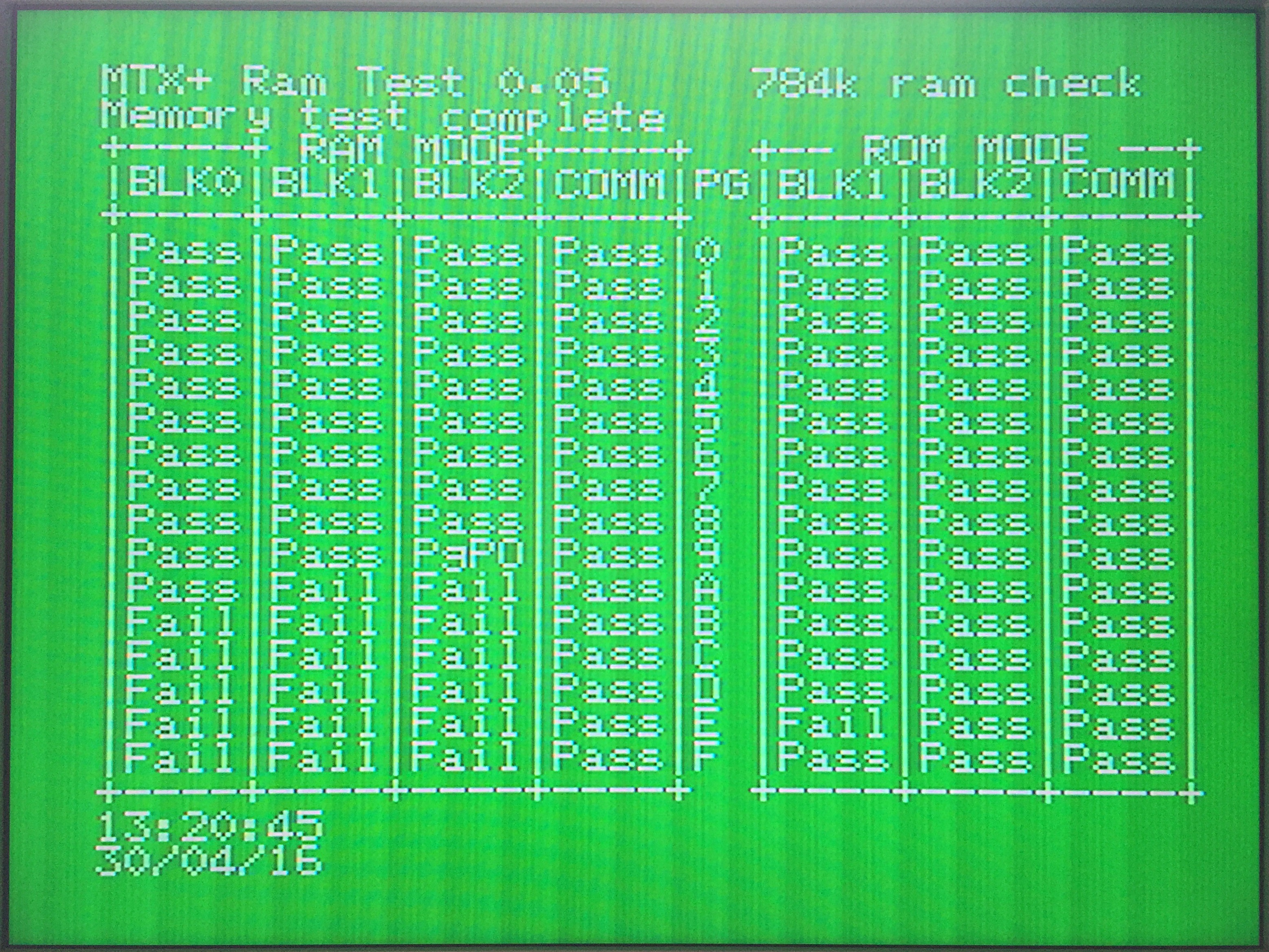
 |
This test reads and
displays the Date & Time from the RTC.
The
RTC being used here had already been set up in the
Z80 CPU board and had the Date & Time programmed,
the values displayed are correct and current -
another good result! |
 |
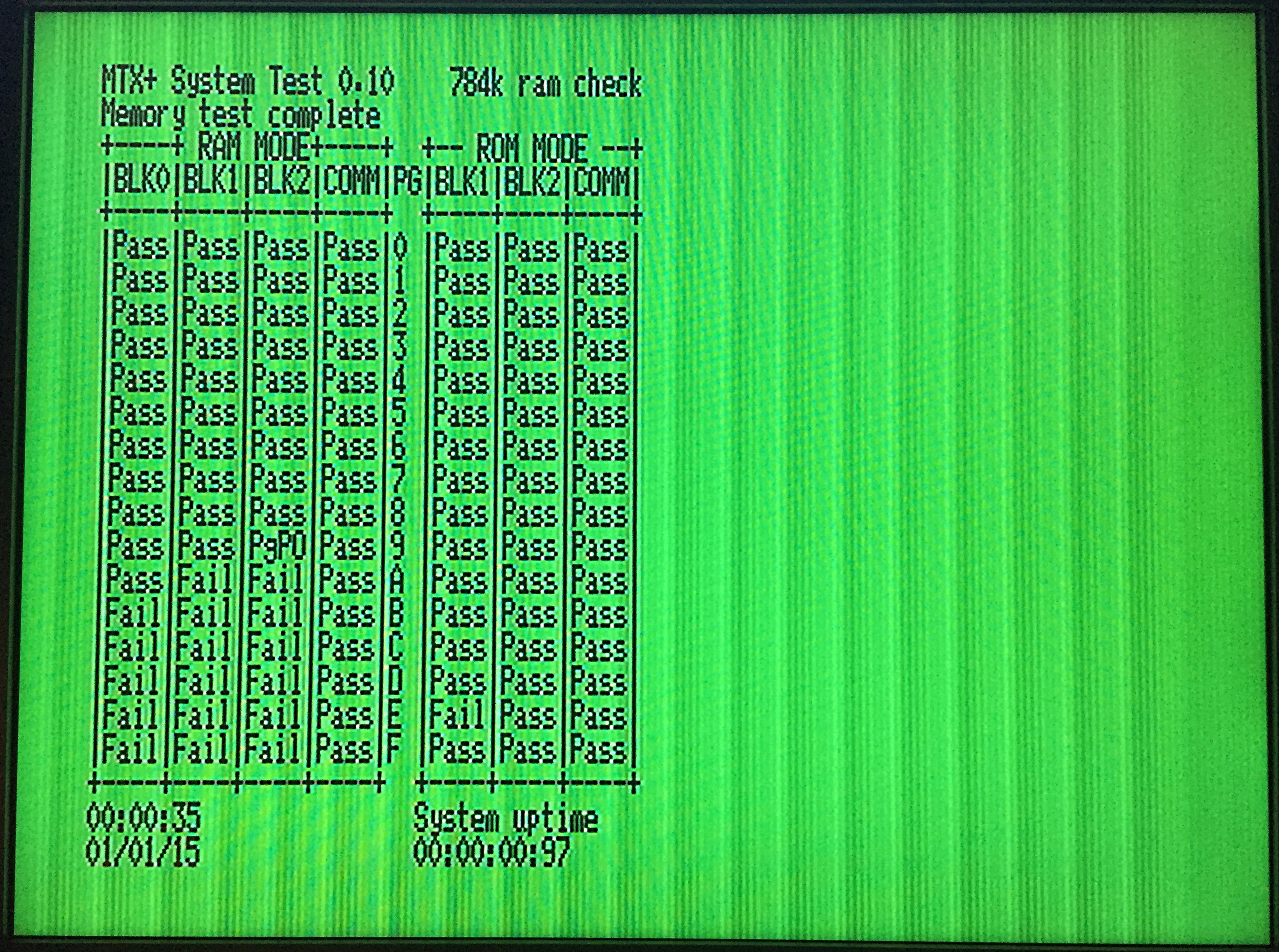
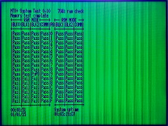
This version of the ROM
should exercise the CTC. As the image shows, the
system appears to "see" the CTC but the "System
uptime" freezes after 0.97 seconds.
The
first issue was there appears to be some conflict
with the CTC when the Diagnostic board is installed,
the CTC counts briefly, then stops. The second issue
was related to how I had wired up the clock on the
board. |
 |
The Z180 features an
internal clock multiplier, which is capable of
running the CPU at twice the input clock speed. My
original V3 design used the clock signal generated
by the CPLD to feed the CPU clock input (EXTAL), the
CTC clock input (PHI) and the backplane PHI signal.
To keep peripherals synchronised with the CPU
clock, the system PHI signal should be driven by the
CPU's PHI output. With the Diag board removed and
the clock signal rewired, the CTC now also runs. |
 |
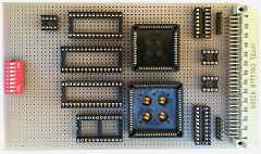
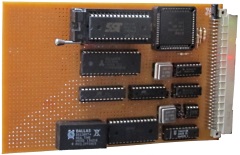
With (almost) all of the
components and sub-systems tested, this is how the
"finished" board looked.
The one missing
component is a 74HC193, used to divide the 4Mhz
clock by 13 to provide the base clocks for the
serial ports. I don't currently have one of those,
but as the serial ports are not currently used, that
isn't really a problem. |
 |
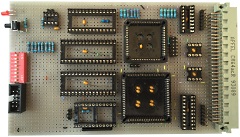
| Component side of Martin's
board |
 |
| |
|
|