|
 |
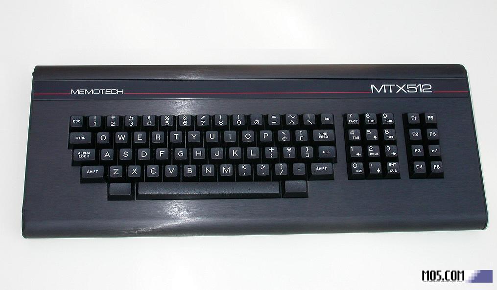
The Memotech MTX Series
|
 |
MTX Series Memory Maps
Overview
The Z80 is an 8 bit processor with a 16 bit address bus,
this allows the processor to directly access a total of 64K
of memory (216 bits). The processor also has a
separate 64K of addresses for input (I) and output (O)
devices. The addresses and data lines for memory and I/O
instructions use the same physical wiring connections, the
Z80 uses different control signals to define when a memory (MREQ)
or I/O (IORQ)
operation is being performed.
| The 64K memory address limit can be extended
using a technique called
bank or
page switching. The operating system can
select which page(s) are addressed at any given
time.
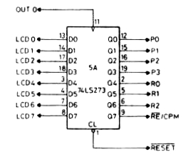
On the MTX computer, the page port,
(Output Port 0), is used to control memory
addressing using the 74LS373 octal latch in
position 5A on the system board. |
 |
|
Page Port Structure
|
Bit |
D7 |
D6 |
D5 |
D4 |
D3 |
D2 |
D1 |
D0 |
|
Function |
RELCPMH |
R2 |
R1 |
R0 |
P3 |
P2 |
P1 |
P0 |
|
|
Mode |
ROM |
RAM |
| Bits D0 to D3 (P0 to P3) |
define the RAM page address |
| Bits D4 to D6 (R0 to R2) |
define the ROM page address |
| Bit D7 (RELCPMH) |
defines a ROM based system (D7 = 0)
, or |
| |
defines a RAM based
system (D7 = 1) |
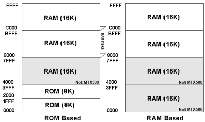
The paged memory map structure of the MTX
computers was designed to operate in two modes,
ROM based (RELCPMH = 0) and RAM based (RELCPMH
= 1).
[Andy has
advised that the acronym for bit 7 is Rom
Enable if Low, CP / M if
High.] |
ROM Based Memory
Map - RELCPMH = 0
When ROMs are enabled,
they are mapped from 0 to 3FFFh. The 8K (2000h bytes)
monitor ROM is always available in area 0 to 1FFFh and
the paged ROMs of 8K (2000h bytes) each are mapped from
2000h to 3FFFh as eight pages 0 to 7 set by R2, R1, R0
in the page port, write only register.
-
Up to 512K of RAM is mapped on 16 pages (0 to F) set
up by P3, P2 ,P1 and P0 in the page port
write only register.
-
The area C000h to FFFFh is a 16K (4000h bytes) block
common to all RAM pages.
-
The 32K (8000h bytes) block from 4000h to BFFFh is
mapped as 16 pages.
-
The 32K bytes of RAM for an MTX500 is mapped from
8000h to FFFFh (page 0).
-
The 64K bytes of RAM for an MTX512 is mapped from
4000h to FFFFh (page 0).
|
R2, R1, R0 |
0000 to 1FFFh |
2000 to 3FFFh |
4000 to 7FFFh |
8000 to BFFFh |
C000
to FFFFh |
Pg |
|
000 |
(0) |
MONITOR
A
(OS) |
SYS B (BASIC) |
512 |
500 / 512 |
500/512
4000h Bytes
Common
Block
|
0 |
|
001 |
(1) |
SYS C (ASSEM) |
(128a) |
512 |
1 |
|
010 |
(2) |
(ROM 2) |
(128c) |
(128b) |
2 |
|
011 |
(3) |
(ROM 3) |
(128e) |
(128d) |
3 |
|
100 |
(4) |
CP/M boot ROM |
(128g) |
(128f) |
4 |
|
101 |
(5) |
SDX ROM |
|
(128h)* |
5 |
|
110 |
(6) |
(ROM 6) |
|
|
6 |
|
111 |
(7) |
CARTRIDGE
|
|
|
7 |
|
(128K Add-on to 64K MTX512
shown in brackets (a-h))
* Note: the diagram in the second (Phoenix)
edition
of the Operator's manual is incorrect, this
diagram is based on the correct position of
block "h" in the original
(Memotech) Operator's manual. |
|
|
8 |
| |
|
9 |
| |
|
A |
| |
|
B |
| |
|
C |
| |
|
D |
| |
|
E |
| |
|
F |
RAM Based Memory Map - RELCPMH = 1
All ROMs are switched out in this mode
and up to 16 pages of 48K (C000h bytes) are mapped from
0 to BFFFh. These pages are set by P3, P2, P1 and P0 in
the page port write only register. In the
area C000h to FFFFh is a 16K block (4000h bytes) of RAM
common to all pages.
|
0000 to 3FFFh |
4000 to 7FFFh |
8000 to BFFFh |
C000
to FFFFh |
P3, P2, P1, P0 |
| 512 |
512 |
500/512
|
500/512
4000h Bytes
Common
Block
|
0000 |
(0) |
| (128a) |
(128b) |
(128c) |
0001 |
(1) |
| (128d) |
(128e) |
(128f) |
0010 |
(2) |
| (128g) |
(128h) |
|
0011 |
(3) |
| |
|
|
0100 |
(4) |
| |
|
|
0101 |
(5) |
| |
|
|
0110 |
(6) |
| |
|
|
0111 |
(7) |
| |
|
|
1000 |
(8) |
| |
|
|
1001 |
(9) |
| |
|
|
1010 |
(A) |
| |
|
|
1011 |
(B) |
|
128K Add-on to |
64K MTX512 |
in brackets (a-h) |
1100 |
(C) |
| |
|
|
1101 |
(D) |
| |
|
|
1110 |
(E) |
| |
|
|
1111 |
(F) |
Further details of MTX computer
memory can be found on these pages :-
MTX Memory
Notes
MTX Memory
Control Overview
<
Previous Page
Goto Next
Page > DRAM Overview
Credits
Information on this page taken from the
Phoenix MTX
Operators Manual.
|