|
 |
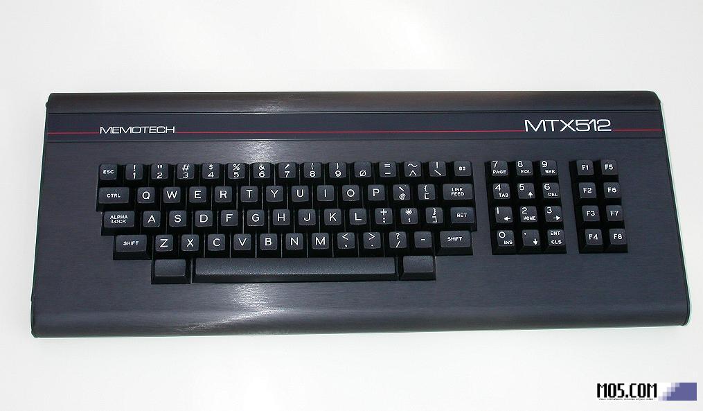
The Memotech MTX Series
|
 |
Z80 DRAM Interface
|
 |
|
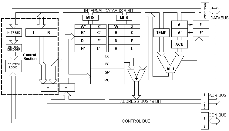
Z80
Processor Architecture |
Z80 Processor Memory Control
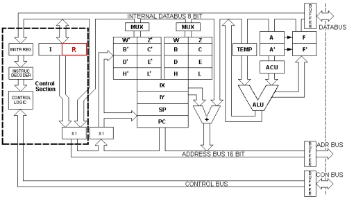
| Architecture The Z80 Processor Architecture diagram
above, shows the internal structure of the Z80,
including its connections to
the external Address, Data and
Control busses and its internal registers.
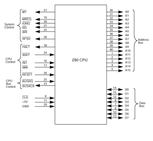
The pin-out of the Z80 is as shown, the most
relevant signals for memory operations are :-
-
MREQ = Memory Request
-
RFSH = Memory Refresh
-
RD
= Read Data
-
WR
= Write Data
|
 |
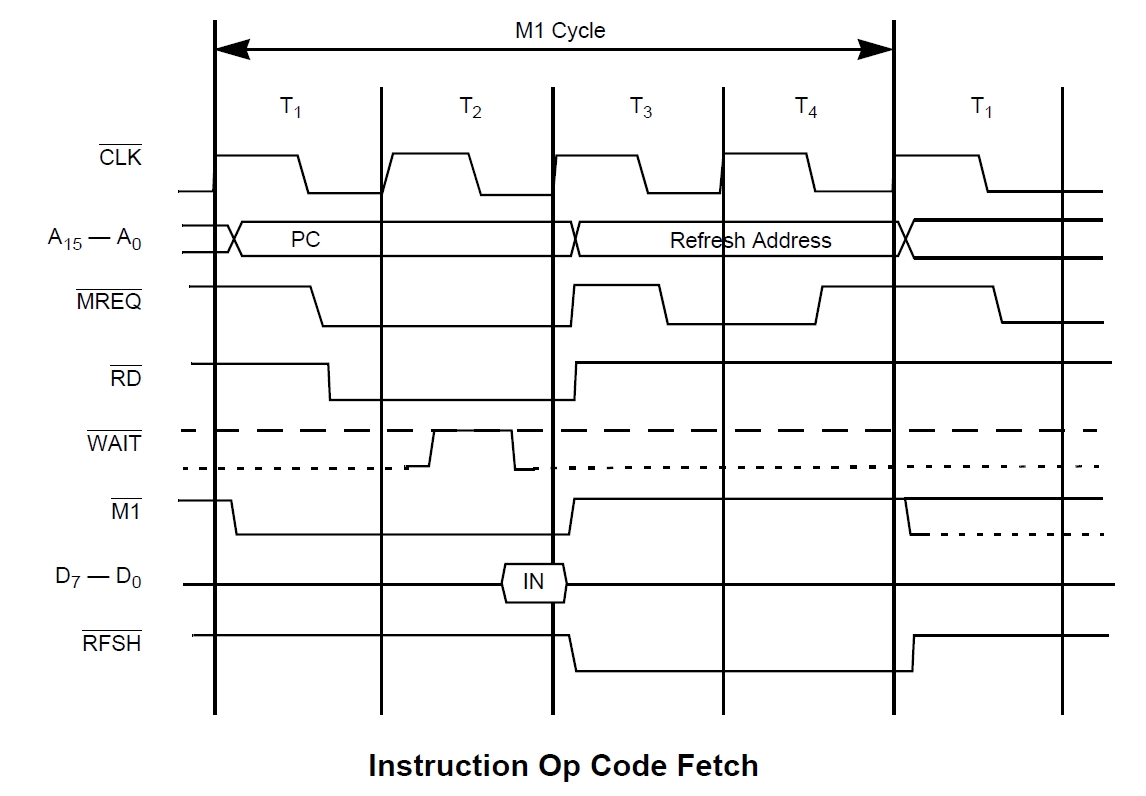
Memory Access
The timing diagram from the
Z80 Databook shows how these signals are sequenced
during RAM read or write operations :-
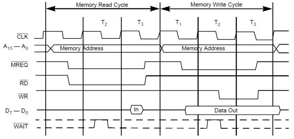
Prior to a memory read or write operation, the Z80 processor
sets bits A0 to A15 of the address bus
to contain the target memory address.
MREQ is the Memory Request signal from
the Z80, this active low signal indicates that the
address bus now holds a valid address for a memory read, write,
or refresh operations (see below).
Read or write operations are controlled using the
RD
and
WR
signals; these active low signals set the direction of data
transfer.
The Z80 does not need to know the physical structure of the
RAM, it is the responsibility of the RAM and other support
chips to decode the address and identify the target memory
cell. The RAM in Z80 based computers, including the MTX
500/512/RS128 computers use
RAS /
CAS
multiplexing, as described on the
previous page, in order to
identify the target memory cell for data transfer between
the Z80 and RAM.
DRAM Refresh (RAS
only Refresh) The Z80 processor includes an "on-chip" memory controller
which controls the Refresh register (R), the
active low output,
RFSH, and the address lines to provide functionality
that can be used to control
the refresh of connected DRAM. (When the Z80 was first
released, this was a major advantage over other
microprocessors of the time that required additional
external circuitry to control DRAM refresh.)
The
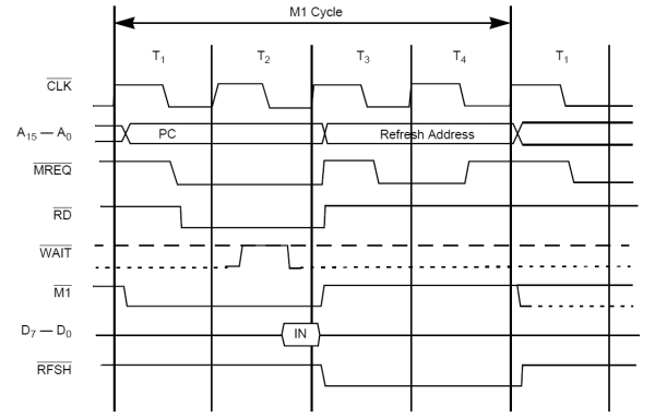
Z80 Databook describes how the refresh signal is
sequenced during an M1 (opcode fetch) cycle. "Clock
state T3 and T4 of a fetch cycle are used to refresh
dynamic memories. The CPU uses this time to decode and
execute the fetched instruction so that no other
operation could be performed at this time. During T3 and
T4, the lower seven bits of the address bus contain a
memory refresh address and the RFSH signal becomes
active indicating that a refresh read of all dynamic
memories must be accomplished. during an M1 (opcode
fetch) cycle". An internal counter increments the lower 7 bits of the
R register that can be used to initiate the
refresh up to 128 rows in the RAM chip, the register is
incremented after each instruction fetch. In the MTX
500/512/RS128 computers, the
RFSH control signal indicates that the lower 7 bits
of the address bus contain a DRAM row refresh address and the
current Memory Request signal,
MREQ, should be used to do a memory refresh for all
DRAMs without waiting for an associated CAS
strobe to target a specific memory cell for Read or Write
operations.
The timing diagram from the
Z80 Databook shows how the
RFSH signal is sequenced during an opcode fetch
cycle:-
Z80 Refresh "Limitations"
As described above, only 7 bits (0 to 6) of this the
R register are used - a throw back to when 16k RAM chips were the norm
and were laid out in a square matrix of 128 x 128 cells, 7
bits were enough to access each address in a matrix of that
size (27 = 128).
If a RAM chip only used the Z80 R register
to refresh its memory cells, the maximum RAM size available
to the Z80 would be 16kbytes, i.e., a matrix of 128 x 128
memory cells for each bit in an 8 byte data word. However,
there are various methods for getting around this apparent
limitation, as described
previously, by laying out the memory cells in a
rectangular, rather than square fashion, for example by
arranging a 64k RAM as a 128 x 512 matrix, the Z80 would be
capable of providing refresh control for 64k RAM as used in
the MTX512 which would be refreshed at the same rate as a
16k, 128 x 128 matrix.
Other methods include adding additional hardware, for
example, monitoring the A6 address line during refresh
cycles and using its transitions to drive an external
counter to drive the A7 line, or even ignoring the Z80
address lines altogether and building a complete external
refresh circuit based on just using the
RFSH signal.
However, as RAM capacity grew, the RAM manufacturers
included additional functionality within the RAM itself such
that 7 address lines could be used to generate refresh of
larger size memories. For example, the OKI 3764, 64k x 1
RAMs used in the MTX512 are divided into two halves, each
half having 128 rows x 256 columns and the refresh address
is used to refresh both halves of the RAM simultaneously.
A key parameter from the
OKI 3764 data sheet, is related to refresh, "128 refresh
cycles / 2ms", this confirms that the RAM will operate
correctly with the Z80's 7 bit counter. Other datasheets
state the same values, often referring to them as "16k
compatible" (e.g. Motorola) or "4116 compatible" (e.g.
Mitsubishi).
The TI datasheet for the
TMS4164
states that the RAM is pin-compatible with the 4116 but also
advises that the refresh requirements are 256 rows in 4ms. I
infer from this that a TMS4164 would not work in a Memotech
computer as the higher rows would not be refreshed. This is
interesting as both the OKI and TI datasheets site the
other's RAM as compatible. I'd be happy to be corrected on
this point though?
The specifics of DRAM access for Read,
Write and Refresh in the Memotech MTX
computer are briefly discussed on the
Next Page. and the essential
DRAM control signals generated by the MTX are described on
Page 3.
DRAM Overview <
Previous
Page Goto Next
Page > MTX DRAM
Operation
|