|
 |
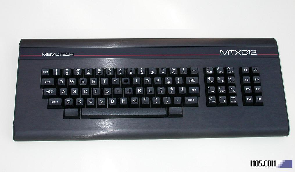
The Memotech MTX Series
|
 |
MTX DRAM
Operation
MTX 500/512/RS128
To understand how the RAM in an MTX 500/512/RS128
computer works, including how the RAM differentiates between a
Refresh cycle and a Read or Write operation, it is useful to
refer to the timing diagrams for the
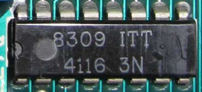
OKI MSM3764 RAM as used
in the MTX512.
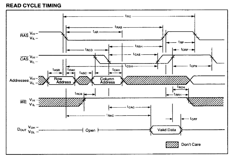
It can be seen from the Read Cycle diagram that for a
Read operation (Write is similar), the
RAS
signal transitions from High to Low for a defined
period, tRAS,
for a Read command to be executed, the
CAS
signal must also transition from High to Low before the end
of the
RAS
strobe.
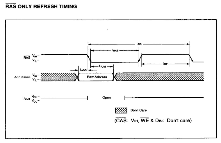
For a DRAM Refresh operation, the
CAS
transition is absent and the RAM interprets the
RAS only strobe as an instruction to refresh the
row referenced by the lowest 7 bits on the address bus.
As described on the
previous page, by arranging a 64k RAM as a 128 x 512
matrix, or, in the case of the OKI MSM3764, by arranging the
memory calls as two "halves", each having a 128 row x 256
column structure and refreshing them at the same time, the Z80 is capable of addressing 64k RAM chips as
used in the MTX512, and these are refreshed at the same
speed as a 16k RAM would be.
The essential memory control signals generated by the MTX
are described on the Next Page.
MTX 512S2
As described on the
previous page, applying the
RAS only
method of memory refresh using the Z80 processor's internal
refresh controller/counter only provides for row addresses
in the 7 bit range, i.e., 0 to 12710 bits or 12810
rows. This is fine for RAM such as the MSM3764 used in the
MTX512, this RAM uses 128 refresh cycles to refresh all rows
in the RAM.
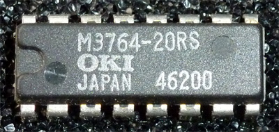
However, larger RAMs such as the MSM41256 or the TMS41256
used in some MTX512S2 computers, require 256 refresh cycles
to fully refresh the DRAM, requiring an 8-bit counter -
beyond the limit of the Z80's internal refresh counter.
Installing 256K RAM on the MTX computer board and using
RAS only
refresh, Memotech would have had to make significant
modification to the memory circuit to provide for an 8 bit
counter.
However, 256K memories also support the
CAS
before
RAS addressing technique.
In this method, the refresh counter is internal to the DRAM
and the address bus inputs are not used, i.e., the RAM has
an on-chip refresh capability.
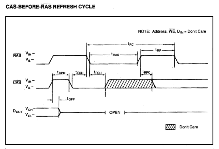
As the timing diagram for a MSM41256 RAM shows, the
CAS
signal goes low before
RAS
and the RAM uses this sequence of events, along with
its internal counter to refresh the required memory cell
row.
Small modifications to the MTX computer board are
required to support
CAS
before
RAS
refresh but the modification are much simpler than creating
an 8 bit refresh counter would have been.
The modifications,
(discussed later),
along with the changes to support the additional address
line required to address 256K of RAM (A8) are
visible by the jumper wires soldered to an MTX512S2 computer
board.
Z80 Processor DRAM
Interface <
Previous
Page Goto
Next
Page > MTX
Memory Control Signals
|