|
 |
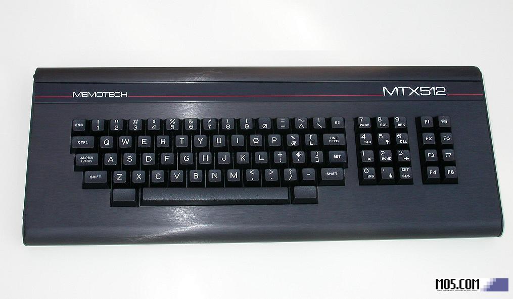
The Memotech MTX Series
|
 |
MTX Series ROM Control
Disclaimer
This information on this page is based on my limited
understanding of the subject, aided by discussion in the
Facebook MTX500 Group with contributions from the likes of
Tony Brewer and Andy Key - any errors are all mine though - if you spot any, please let
me know.
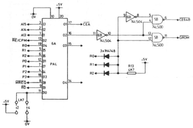
ROM Enable Controls (For a
4000-04 system board with 16K and 8K ROMs)
The MTX computer board could support a number of
different ROM configurations, and used a number of links
close to the VDP to configure the ROM hardware. Details of
the ROM link selection options are shown on my
ROMs page. Selection of the
installed ROMs was controlled by the PAL programming.
Output O1 -
CEA
Output 1 (pin 17) of the PAL is named
CEA,
(chip enable A),
and controls the output enable status of ROM
"A", the 16KB combined OS and BASIC ROM, by setting the
value of OE
of the ROM (pin 22) low to enable the ROM to
write its memory data to the data bus when appropriate.
The PAL logic enables the output when the following
conditions are met :-
- The system is running in ROM mode,
- The CPU has made a memory request,
- It is a read data request,
These inputs are combined with the two cases when we want this
ROM to be enabled :-
- The memory address is in the address space of the
fixed (OS) ROM, 0-1FFFh (0-819110)
- i.e.,
A13 (2^13 =
819210),
A14
(2^14 = 1638410)
and
A15 (2^15 = 3276810)
are all low
- The memory is in the same address space and ROM Page
0 (BASIC) has been selected,
- i.e., R0, R1 and
R2 are all low and the BASIC ROM has been
paged into 2000h-3FFFh (819110
- 1638310)
Leading to the PAL equation :-
|
CEA = |
RELCPMH
*
MREQ *
RD
*
A13 *
A14 *
A15 |
|
+ |
RELCPMH
*MREQ
*
RD *
A13 *
A14 *
A15 *
R0 *
R1
*
R2 |
Output O2 -
CE64B
Output 2 (pin 16) of the PAL does not have a named signal
as it leaves the PAL, but it is the
CE64
element of the signal which has logic applied to it outside
of the PAL to control the output enable status
of ROM "B", the ASSEM ROM and to drive the enable logic for
GROM,
the "GAMES" ROM.
The PAL logic enables the output when the following
conditions are met :-
- The system is running in ROM mode,
- The CPU has made a memory request,
- It is a read data request,
These are combined with the two cases that we want the
CE64
signal to be active :-
- ROM Page 1 (ASSEM) has been selected, i.e., R0,
R1, R2 = 001,
and when
- ROM Page 7 (GAMES) has been selected, i.e., R0,
R1, R2 = 111
Leading to the PAL equation :-
|
CE64 = |
RELCPMH
*
MREQ *
RD
*
A13 *
A14 *
A15 * R0 *
R1
*
R2 |
|
+ |
RELCPMH
*
MREQ *
RD
*
A13 *
A14 *
A15 * R0 *
R1 * R2 |
ROM 1 or ROM 7 Select
Outside of the PAL, the output O2 active low
signal is inverted and forms one of the inputs to the two
NAND gates which drive the ROM "B" chip enable
signal (CE64B)
and the "GAMES" ROM enable signal (GROM).
The way that resistor R13 (4.7k) and the three 1N4148
diodes works is as a wired AND gate. If R0, R1 and R2 are
all logic high (logic 1), none of the three 1N4148 diodes
will conduct and resistor R13 (4.7k) will pull input pin 9
of inverter 6B (74LS04) and input pin 12 of NAND gate 5B
(74LS00) high. This will disable the ASSEM ROM and the
enable signal of the GAMES ROM will be controlled PAL output O2.
If either R0, or R1 or R2 go low, one (or more) of the
three 1N4148 diodes will conduct, which will pull pin 9 of
inverter 6B (74LS04) and input pin 12 of NAND gate 5B
(74LS00) low. So the /GROM output can only go active if R0,
R1 and R2 are high and the output O2 from the PAL (6A) is
low. [Thanks to Mark Kinsey for this
explanation.]
RAM Control Logic
The RAM control functions are described on the
Next Page.
MTX
Memory Control Signals <
Previous
Page Goto
Next
Page >
RAM Control Signals
|