|
 |
The Memotech MTX Series
|
 |
MTX Series RAM Selection
/ Decoding

Disclaimer
This information on this page is based on my limited
understanding of the subject, aided by discussion in the
Facebook MTX500 Group with contributions from the likes of
Tony Brewer and Andy Key - any errors are all mine though - if you spot any, please let
me know.
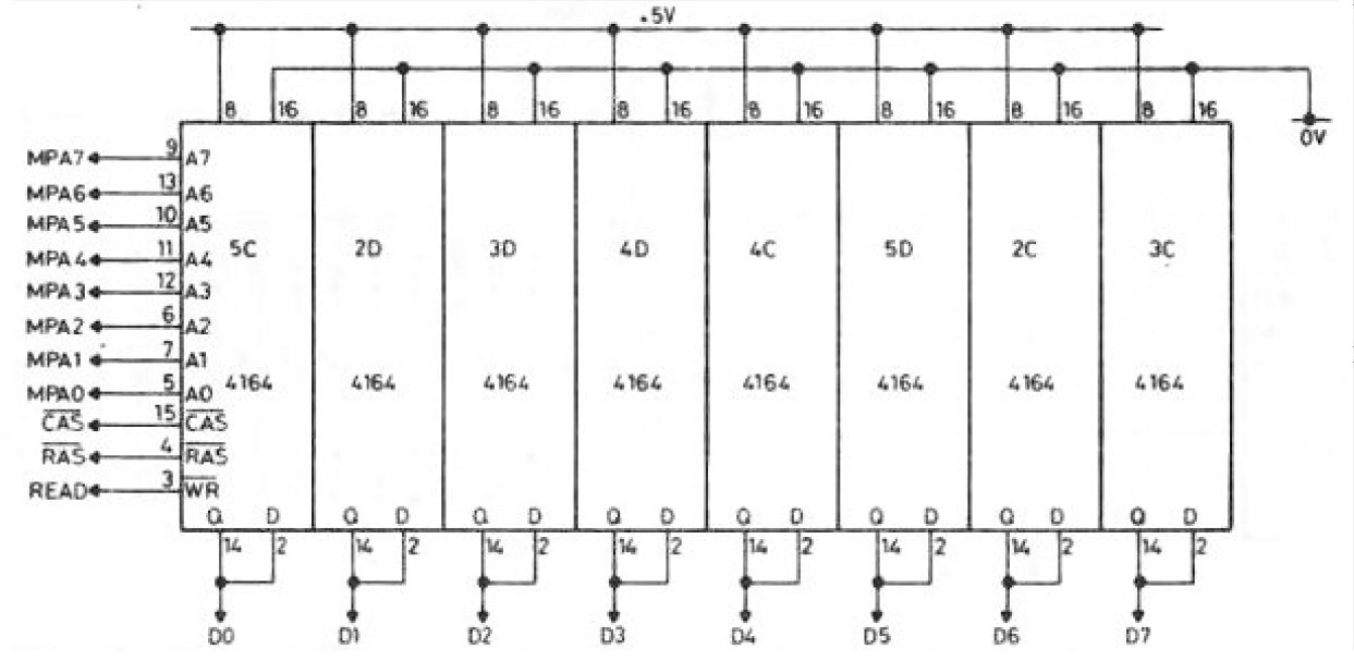
RAM Addressing
As described earlier,
the DRAM in the MTX series of computers uses
address multiplexing, i.e., the same address lines are used to
access the row and column addresses in the RAM by setting them
separately using the Row Address Strobe (RAS)
and Column Address Strobe (CAS)
signals.
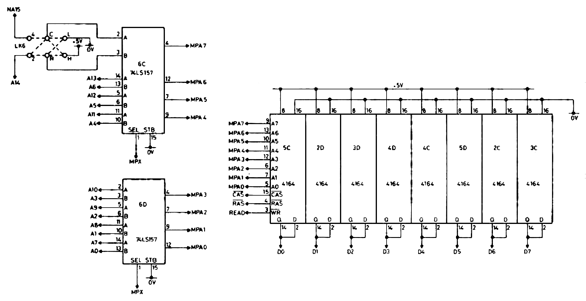
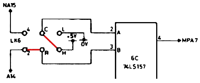
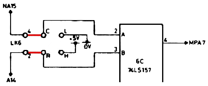
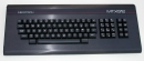
The MTX circuit diagram for the RAM identifies the 8
inputs to the RAM chips as Multi-Plexed
Addresses, MPA0 to MPA7.
The circuit diagram shows how two 74LS157,
"2-Line to 1-Line Data Selector / Multiplexor", ICs are used
to switch the 16 lines of the Z80 address bus onto the 8
MPA lines of the DRAM under the control of the
MPA signal.
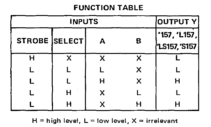
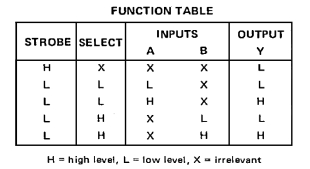
| This is the function table for an LS157, pin
15 (STB) is the strobe
signal (G),
it is an active low signal, tied to 0v for the
MTX, so the outputs are always under control of
the select input (SEL)
on pin 1, coming from the MPA
signal. Therefore, when MPA is
high, the "B" inputs from lines
A0, A1, A2,
A3, A4, A5,
A6 and A14 are passed to the
RAM.
When MPX is low,
the "A" inputs are selected
instead. |
 |
For memory read / write operations, the
MPX signal is used to switch the row and
column addresses to the RAM when required by the RAS
and CAS
signals, as shown on the OKI RAM
timing diagrams, the row addresses are passed first
and the column addresses after a short delay. If only a memory refresh is required, then
CAS
is held high by the
RFSH
signal.
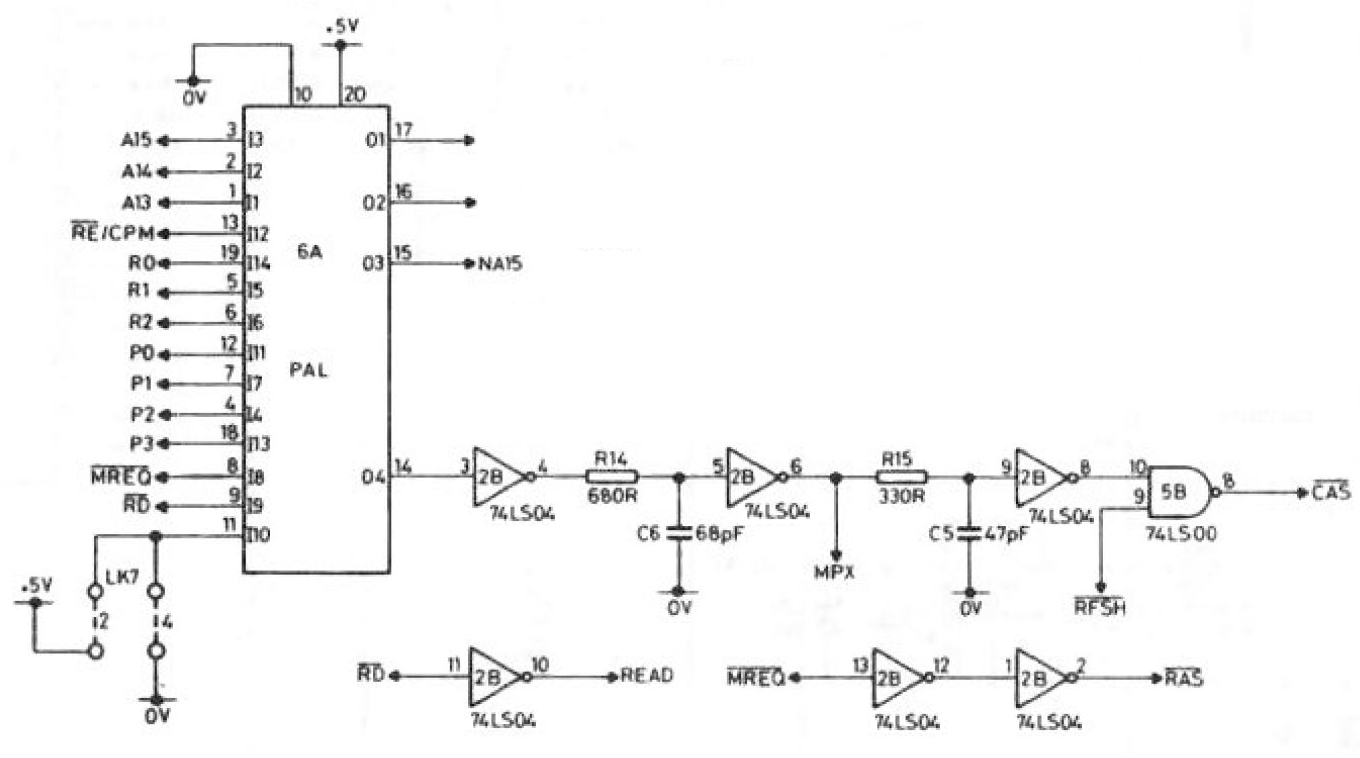
PAL RAM Control and Address Decoding Logic

The PAL circuit diagram shows how the RAS
and CAS
signals are derived as well as the other PAL inputs and
output used to control memory addressing.
Outputs O3 and O4 are used
during a memory operation (read, write or refresh) to
determine whether the address currently on the Address bus
is located in the computer board RAM (rather than on an
external memory board etc.), i.e., we are reading or writing
the onboard RAM and need to sequence the CAS
control signal (subject to the refresh signal,
RFSH).
The
Memotech
MTX500/512 Service Manual describes the purpose of the
computer board links associated with the different RAM
options, this information helps understand the PAL logic
described below.
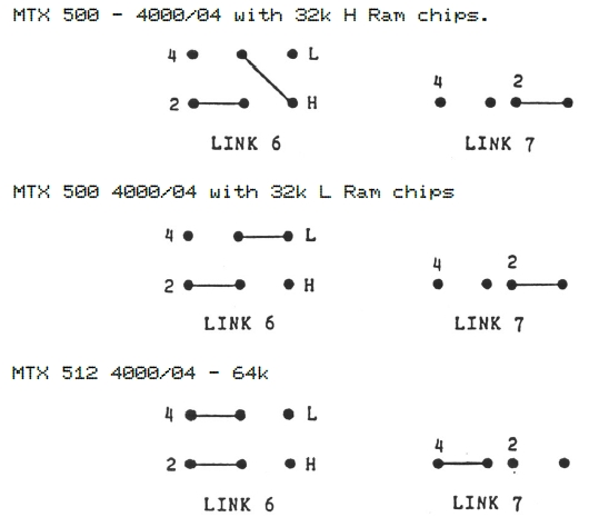
Link LK7
Link LK7 was intended to identify the installed RAM as either 32kbytes (Link 7,
position 2 for +5v) or 64kbytes (Link 7, position 4 for 0v).
In the PAL equations documented in the
Phoenix MTX
Operators Manual this
input is referred to as I2H4L (2High
/ 5v, 4Low / 0v).
Andy
Key has studied the MTX memory maps at length and
has concluded that Memotech's original intention was to have
a single PAL program that could correctly address the
memory, regardless of whether there are 2 or 4, 16 kbyte
pages of memory installed on the system board, i.e., whether
it was an MTX500 (position I2, High)
or MTX512 (position I4, Low).
The purpose of LK7 was to support this
aspiration, however, Memotech were unable to complete the
design on this basis and needed to use different PALs for
the MTX500 and MTX512. It appears that the now redundant
I2H4L (Link 7) input in the PAL equations did not
get removed when spitting the logic into separate equations
for the MTX500 and MTX512.
PAL Output O4 - CAS
Control
Control of the Column Address Strobe (CAS)
is initiated by Output 04 (pin 14) of the PAL which is
further conditioned by the logic outside of the PAL. Output
04 (pin 14) is named /RAM in the
PAL equations, this output is TRUE when the memory address
is located on the computer board RAM (rather than on an
external memory board etc.), i.e., we are reading or writing
the onboard RAM and need to sequence the CAS
control signal, subject to the refresh signal,
RFSH.
Refer to the MTX memory maps
for the two memory modes (RELCPMH = 0) and RAM (RELCPMH = 1)
to see which pages are visible for the MTX500 and 512 in the
two modes. The PAL equations determine whether the
referenced memory address is present in the on-board RAM.
MTX500
|
RELCPMH |
0000 to 3FFFh |
4000 to 7FFFh |
8000 to BFFFh |
C000
to FFFFh |
P0 |
| 0 |
ROM |
(empty) |
RAM |
RAM |
0 |
| 1 |
(empty) |
(empty) |
RAM |
RAM |
0 |
The PAL equation in the Phoenix manual for the MTX500 is
given as :-
|
RAM = |
P3
* P2
* P1
* P0
* I2H4L
* RELCPMH *
A14 *
MREQ |
|
+ |
P3
* P2
* P1
* P0
*
A14 *
A15
* MREQ |
|
+ |
A14
*
A15
*
MREQ |
|
+ |
P3
* P2
* P1
* P0 * RELCPMH
*
A14 *
A15
* MREQ
* I2H4L
|
As described above, for an MTX500 with Lk7-2
made, since I2H4L is tied to +5v, I2H4L
equates to false, and the equation
reduces to :-
|
RAM = |
MREQ
* |
[
P3
* P2
* P1
* P0
*
A14 *
A15 ] |
|
+
[
A14
*
A15 ] |
Note : the reduced equations are meant to
convey the sense of the equation, rather than being
correct Boolean algebra
|
P3
* P2
* P1
* P0
|
= |
All RAM page bits are clear, i.e., RAM Page
0 |
|
A14
*
A15 |
= |
The address is in the 8000 to BFFFh range |
|
OR |
|
|
|
A14
*
A15 |
= |
The address is in the common page,
C000-FFFFh |
So,
to clarify, in order to suit the memory map for an MTX500
when RELCPMH = 0, a valid read/write address must be in the
common RAM area, C000-FFFFh, or in the MTX500 RAM in page 0
at 8000-BFFFh. Although it would appear to be possible to
enter RELCPMH=1 mode, it does not seem useful as CP/M
requires 64KB anyway.
MTX512
|
RELCPMH |
0000 to 3FFFh |
4000 to 7FFFh |
8000 to BFFFh |
C000
to FFFFh |
P0 |
| 0 |
ROM |
RAM |
RAM |
RAM |
0 |
| 0 |
(empty) |
(empty) |
RAM |
RAM |
1 |
| 1 |
RAM |
RAM |
RAM |
RAM |
0 |
MTX512 The PAL equation for the MTX512 is
given as :-
|
RAM = |
P3
* P2
* P1
* P0
* I2H4L
* RELCPMH *
MREQ |
|
+ |
P3
* P2
* P1
* P0
*
A14 *
A15
* MREQ
* I2H4L
* RELCPMH |
|
+ |
A14
*
A15 *
MREQ |
|
+ |
P3
* P2
* P1
* *
A14 *
A15
* MREQ
* I2H4L
* RELCPMH |
However, for an MTX512 with Lk7-4 made, since
I2H4L is tied to 0v, I2H4L
equates to TRUE, and the equation
effectively becomes :-
|
RAM = |
MREQ
* |
[ P3
* P2
* P1
* P0
* RELCPMH ] |
|
+ [ P3
* P2
* P1
* P0
*
A14 *
A15
* RELCPMH
] |
|
+ [
A14
*
A15 ] |
|
+ [
P3
* P2
* P1
* *
A14 *
A15
* RELCPMH
] |
|
P3
* P2
* P1
* P0
|
= |
All
RAM page bits are clear, i.e., RAM Page 0 |
|
RELCPMH
|
= |
RAM
Only Mode |
|
OR |
|
|
|
P3
* P2
* P1
* P0
|
= |
All
RAM page bits are clear, i.e., RAM Page 0 |
|
A14
*
A15 |
= |
The
address is in the common page, 4000-7FFFh |
|
RELCPMH
|
= |
ROM
Mode |
|
OR |
|
|
|
A14
*
A15 |
= |
The
address is in the common page, C000-FFFFh |
|
OR |
|
|
|
P3
* P2
* P1
|
= |
RAM
Page 0 or 1 (P0 = 0 or 1) |
|
A14
*
A15 |
= |
The
address is in the 8000 to BFFFh range |
|
RELCPMH
|
= |
ROM
Mode |
Again, to match the memory map, the /RAM output must be TRUE
for
-
RAM only mode, all addresses (0000 to FFFFh) and memory
page 0
-
In ROM mode, addresses in the MTX512 range (4000-7FFFh)
-
All addresses in the common block (C000-FFFFh)
-
In ROM mode, addresses in the 8000 to BFFFh range in
memory page 0 or 1
In both cases, the RAM equations return TRUE, i.e., pin 14
is low when a reference is made to memory on
the MTX computer board and we need to read or write the RAM,
the signal is further processed outside of the PAL to insert
the required delay on the CAS
signal (see below).
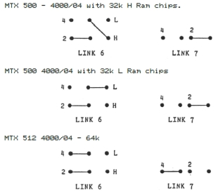
Link LK6
|
In the early 80's, DRAM was
relatively expensive and the yield of fully working
ICs was poor, to keep prices down, the
manufacturers were able to sell half working chips
as functional, but lower capacity, RAMs.
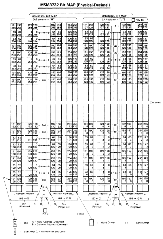
The M3764 has an upper and lower section of 32KB;
chips that had failed factory testing on only one
half of the chip could be used as 32KB RAMs if only
the working half was selected. |
 |
|
The half that was working is denoted by the suffix
on the chip :-
The "32k" RAMs fitted to
MTX500s had been manufactured as 64k but sold as half
working "H" or "L" 32k RAMs. Link LK6-H/L
was used to select which half of faulty 64KB RAM
chips had been selected for use as 32KB RAM chips in
the associated MTX500.
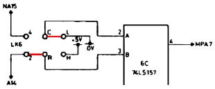
Link LK6-2 is always closed
connecting the MTX A14 address line
to MPA-7 input B, the DRAM
A7 address line.
(Although the three versions of the MTX
motherboard (4000-04, 05 & 06) are individually
described in the service manual, the links are the same for all three
versions.) |
 |
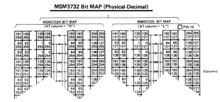
| MTX500 The OKI MSM3732
datasheet states that "Eight row-address bits
are established on the input pins (A0
-A7) and latched with (RAS).
The seven column-address bits (A0
through A6) are established on the
input pins and latched with CAS.
One Column Address (A7) has to be
fixed at logic "0" (low level) for MSM3732L, and
at logic "1" (high level) or MSM3732H."
For an MTX500, the LK6-H/L
positions are set to meet the OKI criteria to
utilise the working half of the RAM - link
LK6-4 is always open so the NA15
line is never selected and an address in the 32K
range of the good half of the RAM is selected
based on the link position. |
 |
 |
| MTX512 The eight column-address
bits (A0 through A7) are
established on the input pins and latched with CAS.
The LK6-H/L position is not used
on an MTX512, NA15 is used to set MPA-7 input A, subject to
the PAL logic. |
 |
PAL Output O3 -
NA15
For both the MTX500 and MTX512,
the NA15 PAL equation in the
Phoenix manual is given as :
|
NA15 = |
A15
|
|
+ |
P3 *
P2 *
P1 *
P0 * RELCPMH
*
A14 *
A15 |
As described above, LK6-4
is never made for an MTX500, and therefore any reference to
it (as NA15) in the
PAL equation is of no value and likely a hangover from
the unsuccessful attempt to have a single MTX computer
PAL.
For an MTX512, NA15 is
used to set MPA-7 input A. and becomes the
MSB of the column address, selecting which half of the
RAM holds the target memory cell.
|
NA15 = A15 |
= |
NA15 output is high when A15
is set, i.e., the memory address is in the
range >=
8000h |
|
OR |
|
P3 *
P2 *
P1 *
P0 |
= |
RAM Page 1 |
|
RELCPMH
|
= |
ROM Mode |
|
A14
*
A15 |
= |
The address is in the 8000h to BFFFh range |
For the first term, if the address is >8000h, then A15
is 1 and
NA15 is FALSE, and as it is
active low, it is = 1, so NA15
= 1
For the second term, with RELCPMH=0, RAM page 1 selected
and the address in the 8000h to BFFFh range, A15
is 1 and A14 is 0, so as
NA15
is TRUE, then NA15 = 0
The OR results in NA15 being
0, so, rather than an address of 8000h to BFFFh being
strobed onto the RAM address lines, a memory address in
the range 0000h to 3FFFh is specified instead. Or,
quoting from
Andy's hardware web page ...
"The NA15 equation remaps accesses in
RELCPMH=0 mode, to RAM Page 1, Z80 addresses
0x8000-0xbfff, to DRAM addresses 0x0000-0x3fff. Put
another way, this is how the δ page moves between
RELCPMH modes."
Discrete RAM Control Logic
(MTX500/MTX512/RS128)
RAS
Control
The Row Address Strobe (RAS)
is controlled out-with the PAL as shown :-
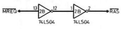
MREQ is the Memory Request signal from
the Z80 processor, this active low signal indicates that the
address bus holds a valid address for a memory operation
(read, write or refresh). The signal passes through two
inverters in the 74LS04 at board position 2B which
introduces a small delay between
MREQ and
RAS, based on the
SN74LS04 datasheet, this is in the order of 20 ns.
The circuit diagram shows that the
RAS signal is strobed on every
MREQ high to low transition, i.e., for every Read,
Write or Refresh. In the quiescent state, the
RAM
signal, PAL output O4,
is high, having been inverted twice, the
MPX signal will also be high and the74LS157
data selectors will have their "B" inputs selected, i.e.,
A0, A1,
A2, A3, A4, A5,
A6 and A14. When
RAS
is strobed, the data on the lines is passed to the RAM and
form the row address of the target memory cell.
If there is not an active memory read or write operation
in progress, the CPU will have set the
RFSH
signal low along with
MREQ to initiate a refresh of the DRAMs using the
lower 7 address bits and the
CAS
signal will stay high.
CAS
Control
The CAS
control signal is controlled by the PAL (see above), but
from a purely timing perspective, behaves as follows :
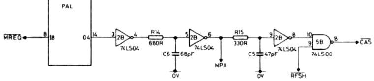
MREQ goes low to initiate the RAM
access, in order to read or write to the RAM, the active low
output on pin 14 goes low if the onboard RAM
is being referenced. Previously, pin 14 of the PAL
will be high, and, having been inverted
twice, the MPX signal will also be high. The
row addresses will have been passed to the RAM first, under
the control of the
RAS signal
described above.
The double inversion and
RC network
are configured to provide the necessary delay to ensure that
the MPX signal has put the column addresses on
the RAM input address lines before the
CAS
signal is generated.
Putting it all together . . . . .
I wanted to understand the effect of different component
values on the relative delays to the
RAS and
CAS
signals and simulation seemed to be the way to do it.
Texas Instruments have a
free
SPICE based simulation program available by
registering on
their website. Quoting from the TI site, "TINA is an
easy-to-use, powerful circuit simulation tool based on a
SPICE engine. TINA-TI is a fully functional version of TINA,
loaded with a library of TI macromodels plus passive and
active models."
My TINA schematic of the MTX RAS
and
CAS
control signals looks like this :-
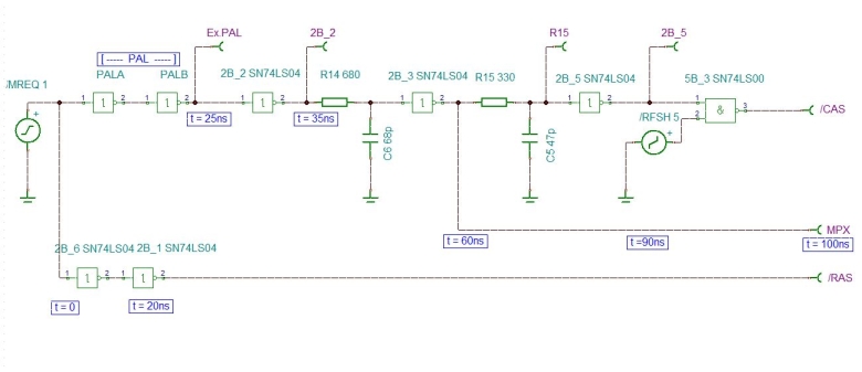
The schematic is drawn a little differently than in the
MTX manual, but it is functionally equivalent. The "PALA"
and "PALB" inverters are there to replicate the time delay
associated with the PAL. The combined effect of these two
gates is to introduce a delay of 25ns.
This is the TINA output from a run from a simulation of
the schematic shown :-
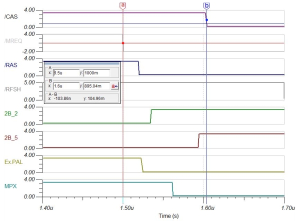
Prior to the CPU initiating a memory access, the address
bus will have been loaded with the target address before
taking
MREQ low. In the simulation run, you can see that the
MREQ goes low at 1.5us (cursor "a") and the two NOT gates introduce
a delay of ~20ns before RAS
goes low to strobe the addresses onto the RAM address
lines. The MPX signal is delayed by a further
~40ns, set by the values in the first RC network, and then switches the other 8 address lines ready for
the
CAS
strobe which follows ~40ns later (cursor "b"), giving an
end-to-end time of ~100ns.
Note: The RAM
CAS
timing described on this page is based on the original
circuit design which will be found in machines shipped
before October 1984. The changes made to machines shipped
after this page are described on the
Overview Page
The modifications required for the MTX512S2 are described on
the Next Page.
ROM
Enable Signals <
Previous
Page Goto
Next
Page >
MTX512S2
|