|
 |
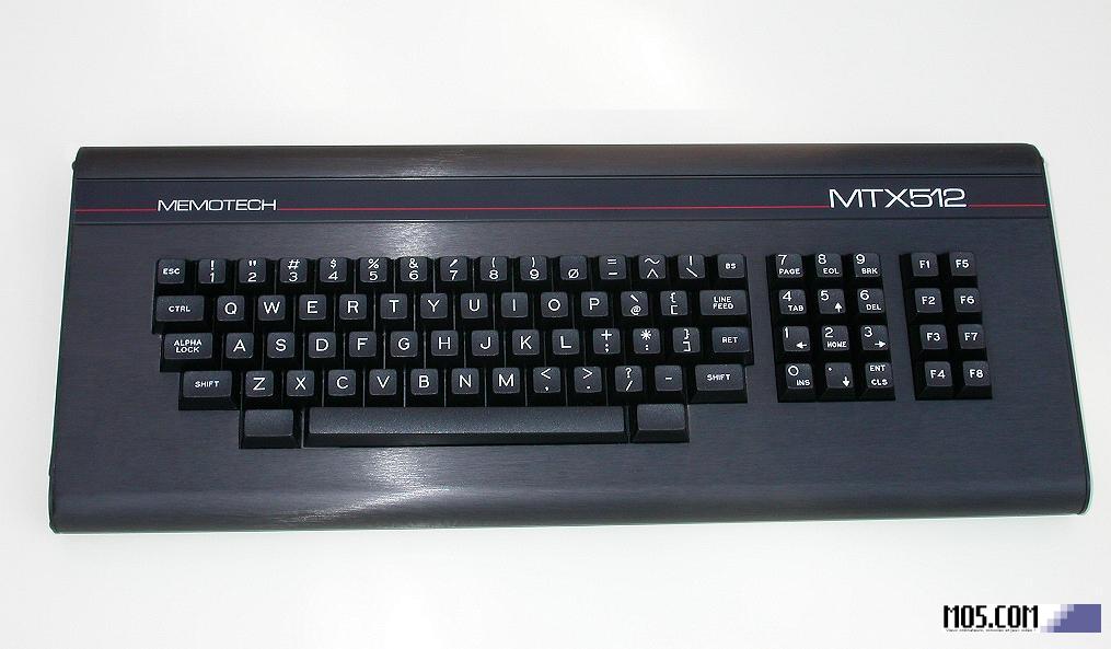
The Memotech MTX Series
|
 |
MTX Series ROM
Configuration

Disclaimer
These pages were written as I attempted to gain a better
understanding of the different ROM configurations used in
the MTX series of computers
The information here will likely evolve as I learn more, but
it is not guaranteed to be
accurate and may contain glaring errors, obvious to anyone
who knows about these things - if you spot any, please let
me know.
ROMs - Overview
|
Motherboard ROM Options
|
Board Version 4000-04
 |
Board Versions 4000-05 &
4000-06
|
| ROM |
Location |
Size |
Function |
ROM |
Location |
Size |
Function |
| A |
9H |
16KB |
OS & |
A |
9H |
8K |
OS |
| |
|
|
BASIC |
B |
8H |
8K |
BASIC |
| B |
8H |
8KB |
ASSEM |
C |
10H |
8K |
ASSEM |
|
| MTX Computers have 24KB of ROM installed on
the system board. The first computers,
using the 4000-04 version system board, had a 16KB
combined Operating System (OS) and BASIC language ROM, along with an 8KB
Assembly language (ASSEM) ROM.
Later models, using 4000-05 and 4000-06 version
system boards, had separate 8KB ROMs for each of the OS,
BASIC and ASSEM functions.
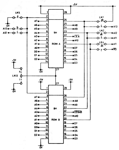
This is a copy of the circuit diagram from
the
MTX Operator's Guide (which is also included
in the Service Manual) for a 4000-04 version
system board.
I am not aware of the ROM hardware
configuration options being documented in any of
the available Memotech literature.
It may be obvious to others, but it took me a
little while to understand it, so I thought I'd
document here in case that it is useful for
others too. |
 |
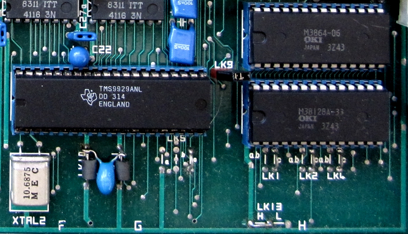
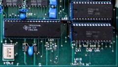
| The ROMs are located
next to the VDP, this photo is of a 4000-04
version computer board. The upper ROM is the 8KB
assembly language ROM (B) and the lower one is
the 16 KB combined Operating System and BASIC
ROM (A). As well as providing for the 2 or 3
ROM option, the board also supported a number of
different ROM types, the motherboard has a
number of link/jumper positions to configure
these options. |
 |
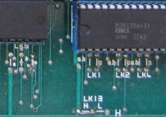
| A close up photo of the link
positions along with an annotated version if you
can't make out the text on the thumbnail or full
size photo. |
 |
 |
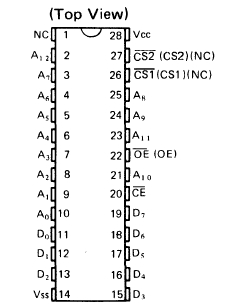
| The best way to describe how the
link options are used is by way of an example.
The pin-outs shown are from a M3864 on the left
and a 2364 on the right.
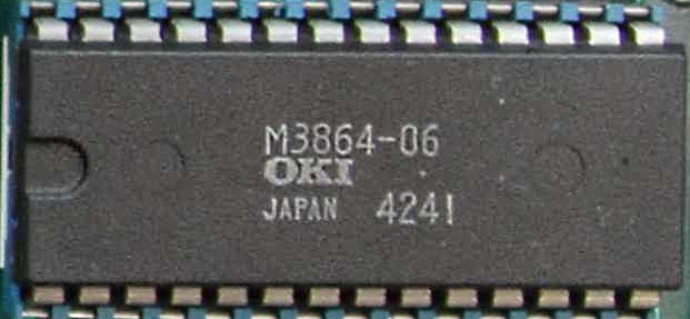
The M3864 is the most common 8K ROM seen
installed as the ASSEM ROM (B) on MTX computer
boards.
The 2364 is an older type of 8K ROM, although
I have not actually seen this type of ROM
installed on an MTX, it does serve to illustrate
the concept. |
 |
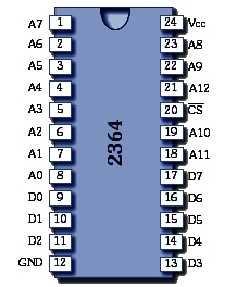 |
| The most obvious
difference between these two types of ROM is the
number of pins on the packages - 28 and 24. The
MTX circuit diagram indicates that 28 or 24 pin
ROMs can be used by a horizontal line between
pins 2 & 3 and 26 & 27, although normally hidden
by the installed ROMs, a similar line and chip
"notches" are also stencilled on the board
itself. It can be seen that the function of
most of the pins are the same, where they are
different, the computer board links can be used
to make the necessary changes.
Power is supplied to a 2364 on pin 24,
the position occupied by pin 26 of a M3864.
Lk1, position "ab"
can be used to put +5v onto this pin (the
M3864 CS1, chip select, function is not
present in a 2364).
|
Similarly, the connection for A12
is made using Lk5, position "c"
for a M3864 (to pin 2) or Lk2,
position "ab" (to pin 21) for
a 2364.
|
The connection for A11 is
made using Lk2, position "c"
for a M3864 (to pin 23) or Lk4,
position "ab" (to pin 21) for
a 2364 (the M3864 chip enable
function controlled by connecting
RD to pin 20 using Lk4,
position "c" is not present in
a 2364).
|
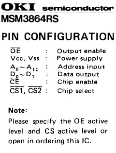
| For a ROM such as
the M3864 which has two chip select inputs, both
must be active for the outputs to be enabled and
the 8-bit data value to be read, when either
signal is not active, the outputs are in the
high impedance state, i.e., disconnected from
the data bus. As this extract from the 8KB OKI
M3864 ROM datasheet shows, the ROM could be
specified to have active high or active low
output enable and chip select
pins, OE /
OE and CSx /
CSx.
As the circuit diagram shows, for an M3864,
using link Lk1, position "c",
CS1 is controlled by A13.
Although the CS2 function is not used for the
MTX, to enable the outputs, the CS2
pin must be active by holding it at the required
voltage level. Lk13 is set to hold
the signal high (5v) or low (0v) as required. In
the case of the example shown, Lk13
is set to "H", holding CS2
at 5v. |
 |
|
16KB ROMs |
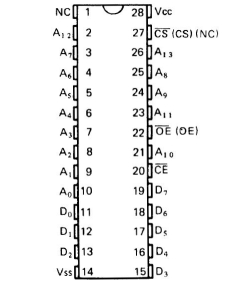
| The pin-out for a
16KB M38128 ROM is shown here, to allow the
additional 8K to be addressed, and additional
address line (A13) is required on the ROM. In
this case, there is only a single chip
select signal and CS2 has
been replaced by A13. For a 16K
ROM, Lk1, position "c" connects ROM pin 26 (A13)
to the A13 address line of the MTX
address bus. |
 |
|
ROM Paging |
| Memory selection for the MTX is
done using the page port (output
port 0), rather than duplicate my explanation of
the page port on this web page,
see this page, (a work in progress), for a
description of the page port
functionality. At this point, it is enough to
know that when ROM mode is enabled, i.e., when
not running in RAM only mode under CP/M, all of
the ROMs are mapped into the 16KB memory address
range from 0 to 3FFFh.
The 8K OS portion of the ROM is always
present at 0000 to 1FFFh, the other ROMs are
"paged" in as required to the address range from
2000h to 3FFFh. |
| R2,R1,R0 |
0 - 1FFFh |
2000-3FFFh |
| 0 |
OS |
BASIC |
| 1 |
ASSEM |
| 2 |
(2) |
| 3 |
(3) |
| 4 |
CP/M Boot |
| 5 |
SDX |
| 6 |
(6) |
| 7 |
"GAMES" |
|
| The ROMs most often
seen in an MTX are OKI M38xxx series, data
output from these ROMs are enabled by the
output enable,
OE,
pin 22. (In a 2364 it is done by the chip
select, CS, signal on pin 20.) In an MTX,
the OS & BASIC ROM (A) is controlled by the
CEA signal on pin 20, and the
ASSEM ROM (B) is controlled by the
CE64B signal on pin 20.
These chip enable signals are
controlled by the memory address decoder PAL
which also controls the DRAM row address
strobe,
RAS, and column address
strobe,
RAS, as well as decoding the RAM
addressing.
For a description of the operation of the
memory controller PAL,
go to this page.
|
Credits
Some information taken from the Memory
Investigation section on Andy's
Memotech Hardware webpage.
|