|
 |
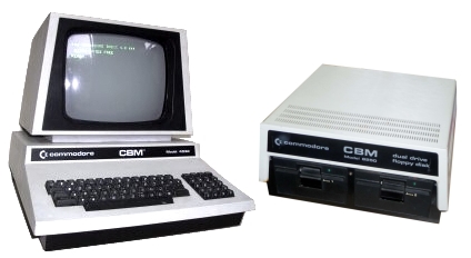
Commodore PET Projects
- petSD+ |
|
petSD+ - Assembly |
 |
 |
|
English |
Deutsch |
Last Firmware Update :
Get it here
Introduction
The original petSD was designed to be constructible by the
average electronics hobbyist, and one of the design
goals was to be able to use through-hole-technology
(THT) components, rather than surface mount chips.
The one exception was the FT232RL USB-serial-adapter
for which a THT equivalent was not available. The
USB - serial adapter has been dropped from the petSD+
design, the only surface mount component remaining
is the SD card reader.
Assembly of petSD+ is relatively straightforward, if you have
reasonable soldering skills and some experience of constructing
electronics projects, then you should have little difficulty
with self-assembly and you can skip to the
assembly details. However, it is probably not a good project
for a novice to start out on.
Before you start to build your petSD+, you should read through
this page and study the photos to satisfy yourself that your
skills are up to it. If you have any doubts about your ability
to follow the steps below and make a reasonable job of building
petSD+, I would strongly advise that you reconsider whether your
should attempt to build it yourself. At the very least, get some
practice with soldering components onto a piece of prototype
board before you take the plunge and have a go at petSD+.
Tools Required
The tools listed here are the bare minimum that you will need,
most hobbyists will have considerably more tools at their
disposal which will likely make construction easier.
| Tool |
Minimum |
Notes |
| Soldering iron |
20-25W
Fine
(conical) tip
No
temperature control
|
A temperature controlled solder station allows
the user to have much more control over the tip
temperature and reduces the risk of damaging the
component or PCB tracks.
In this case, the most sensitive components,
i.e., the ICs, should all be mounted in sockets.
With care, the passive components can be soldered
using a very basic iron with little risk. |
| Soldering iron stand |
A simple
metal stand |
More advanced (i.e., more expensive) cradles may
include lights, magnifying glasses, clamps to hold
the work-piece etc. |
| Solder |
From your plumber ? |
NO !
You need a good quality, electronics grade,
solder. I use 0.7mm diameter, 60% Tin/40% Lead
solder with integral flux.
Due to the
potential health risks associated with
lead,
in recent years, the use of lead based solder in
manufacturing has been phased out (see
RoHS). Lead-free solders are available, but, are
a bit more difficult to work with as they have
higher melting points and don't flow as easily.
When using lead based solder, take sensible
precautions, such as having adequate ventilation.
not breathing in the fumes (that applies to all
solders), etc. |
| Test equipment |
Continuity tester
Preferably with an audible alert (buzzer) |
The first task is installation of the SD card
reader, it is critical that its installation has
been proven before progressing with the build as it
will be almost impossible to correct after the board
has been completed. The minimum requirement is for
a basic continuity tester, but a basic multi-meter
than can measure voltage and resistance is recommended,
particularly if you need to fault-find a non-working
board. |
| Various |
|
Good quality miscellaneous tools, small
side-cutters, long nose pliers, etc. etc. |
Parts Required
If you have purchased a kit of parts for petSD+, or you are
gathering the parts together yourself, make sure that you have
the parts listed on this page.
Notes :
-
Some parts are optional, depending on
whether you need the real time clock or the LCD display and
whether you choose to mount petSD+ internally or externally
to your PET
-
The PCB includes an In-System Programming
(ISP) port for programming the MCU for first use, when the
device configuration "fuses" are set and a boot loader is loaded for the first time.
Once the boot loader has been configured, the application
firmware can be loaded from the SD card. Since the petSD+ parts kit will include a
pre-programmed MCU, the ISP port header will not be included
in the parts kit.
-
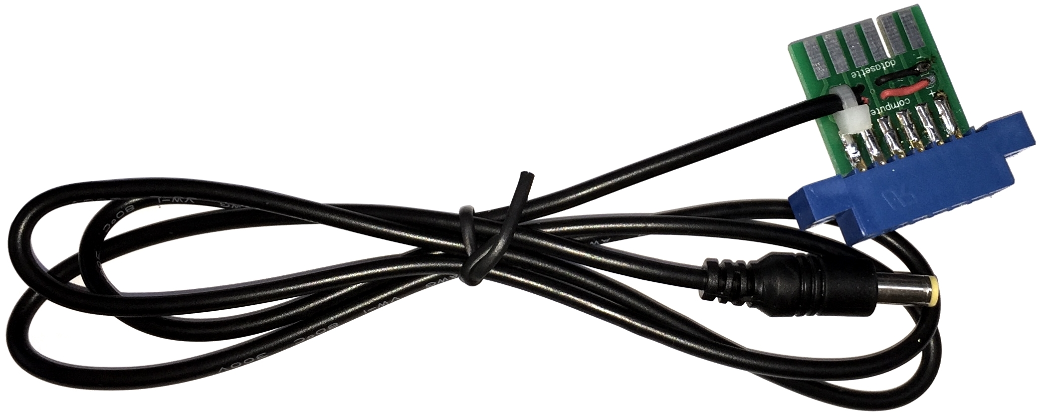
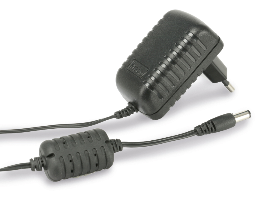
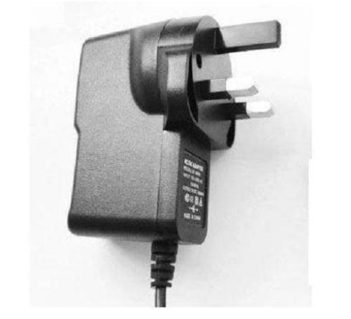
petSD+ requires a +5V power supply for
operation, this can be provided in a couple of ways - either
from the PET cassette port using a custom cable (available
as an additional option), or using a stand alone, "wall
wart", PSU rated for at least 500mA at 5 volts. If
mounted internally, power can be
picked up from a convenient place on the PET PCB.
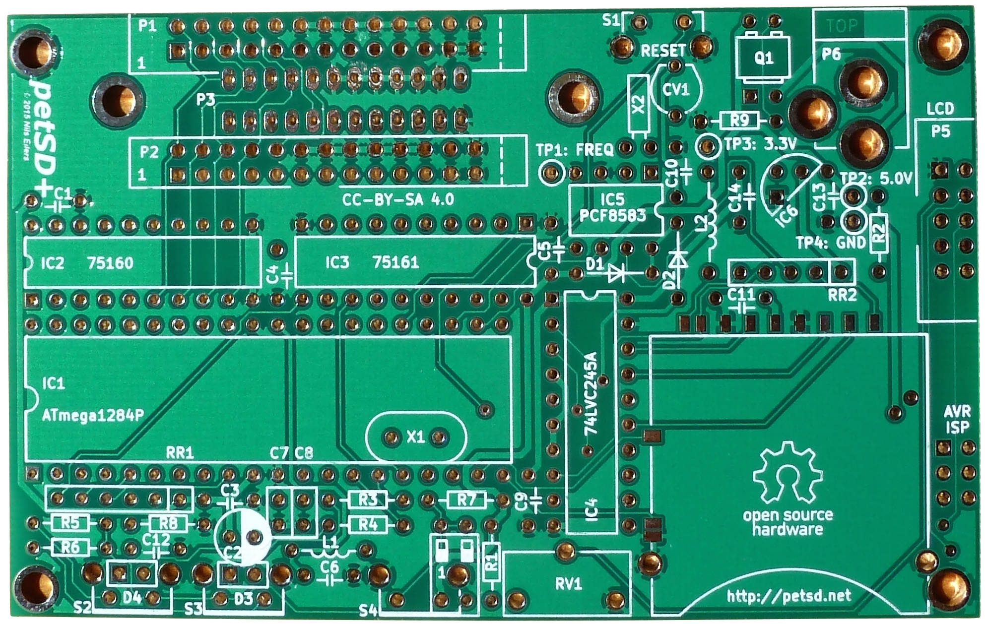
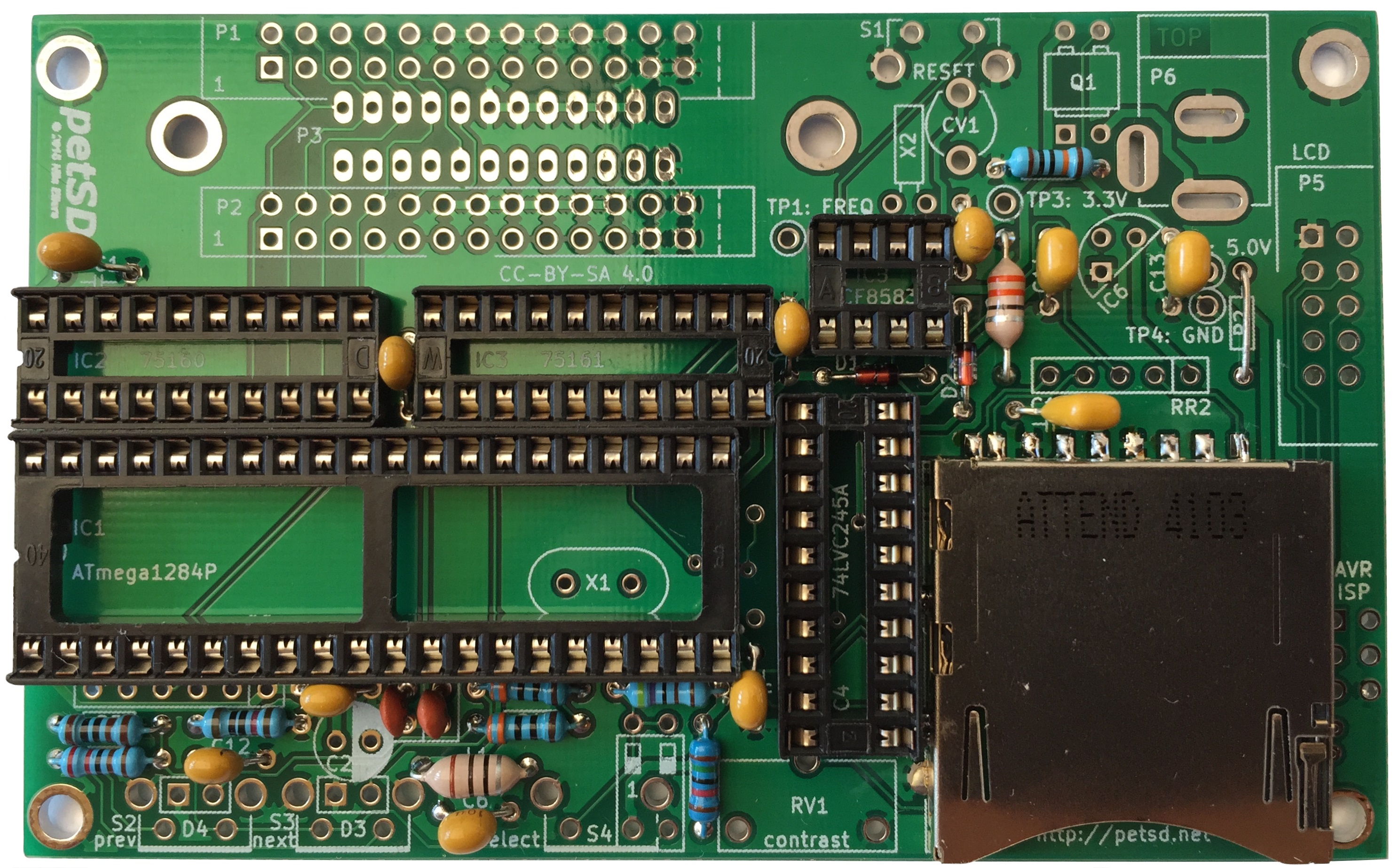
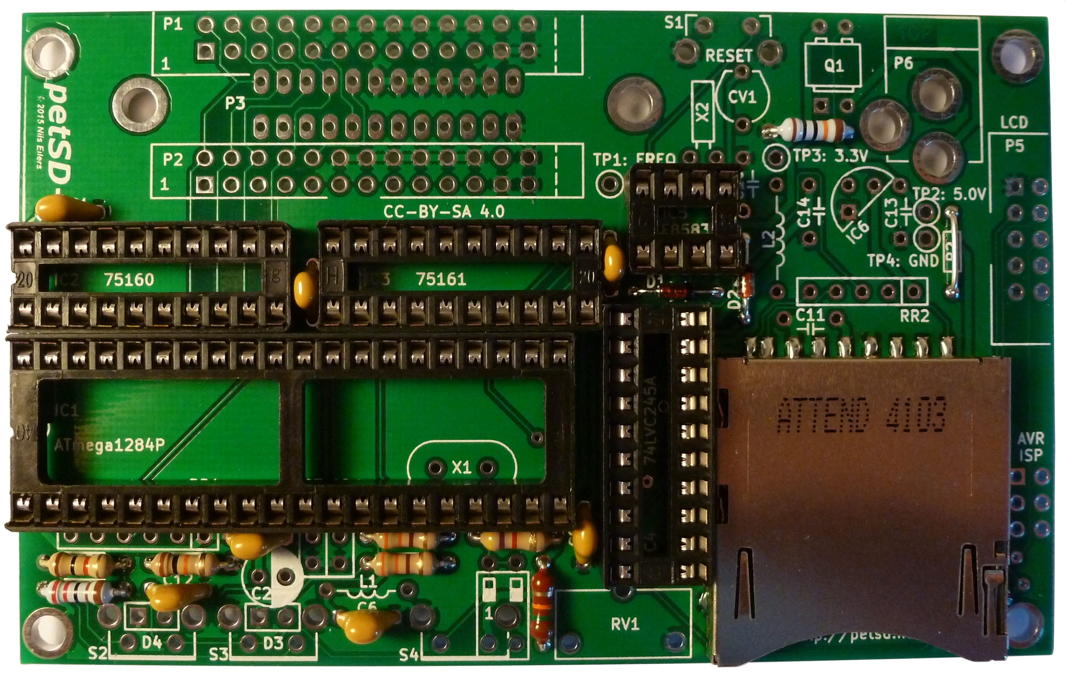
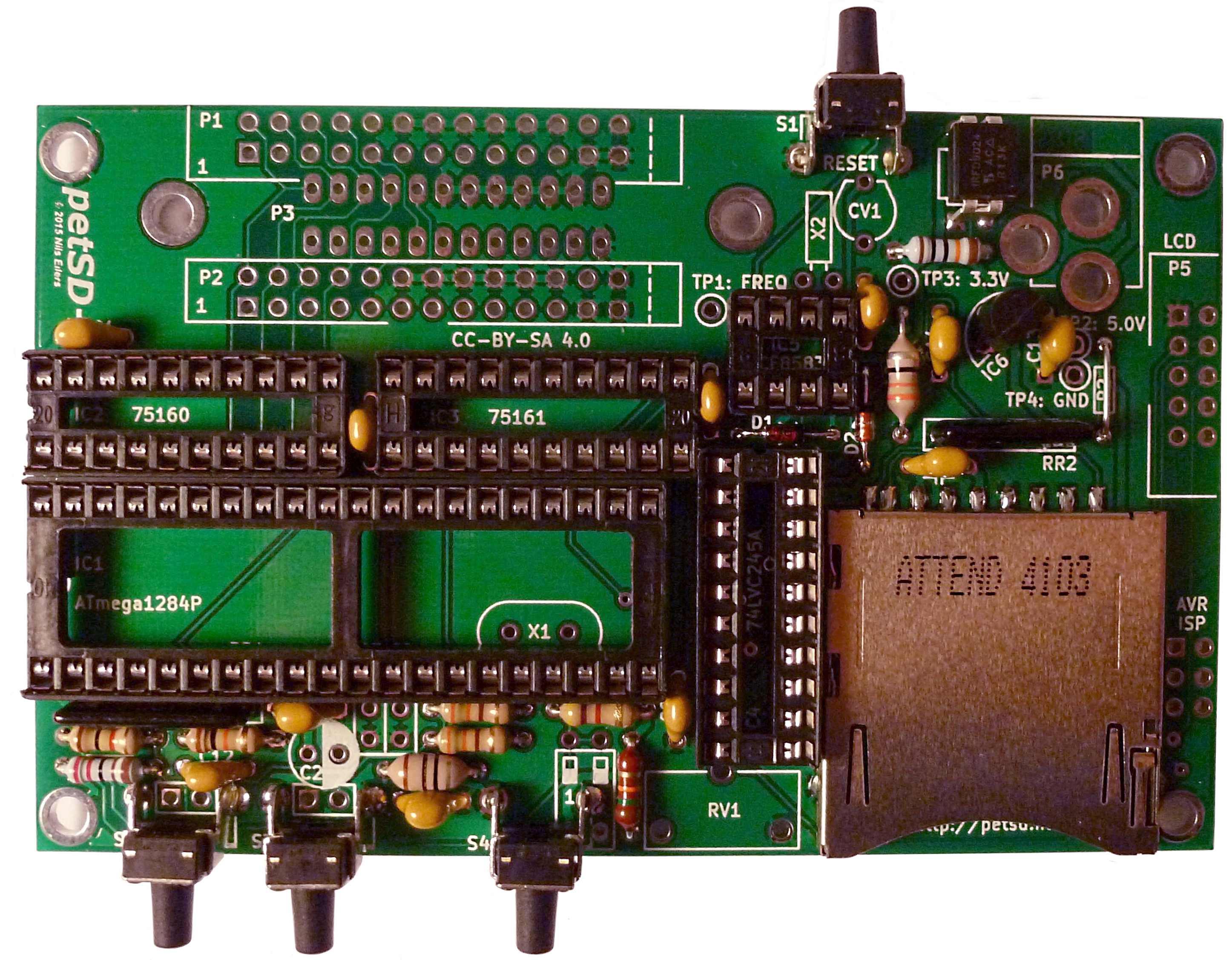
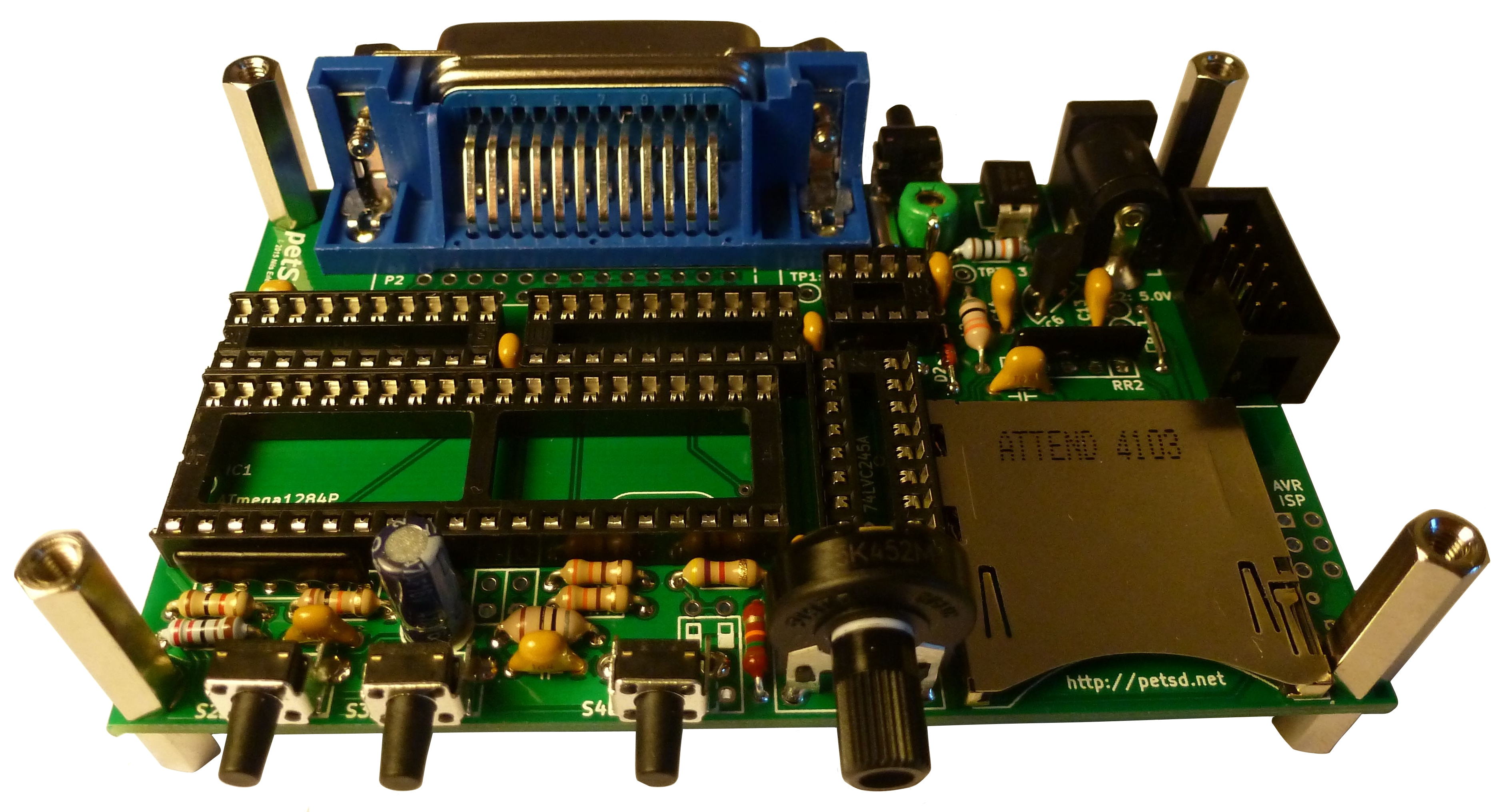
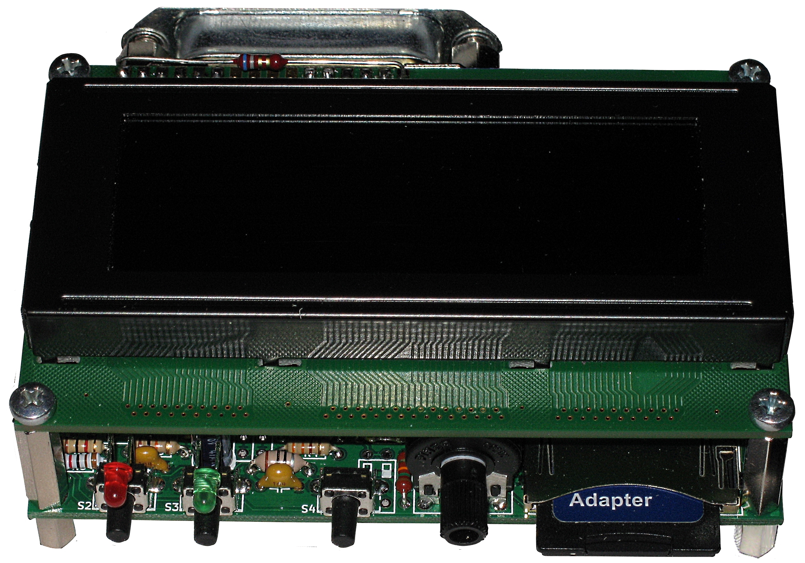
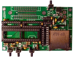
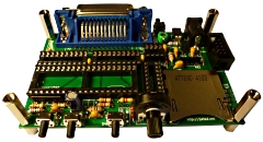
Assembly Instructions - PCB Version 1.1
Older Versions : PCB Version 1.0
 |
 |
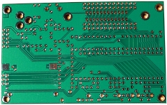 |
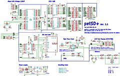
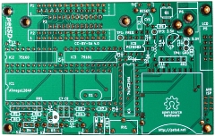
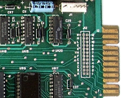
| petSD+ Schematic |
PCB Component Side |
PCB
Solder Side |
| The
parts list includes a suggested order for
mounting the components, with the exception of the
SD card slot, it isn't essential that you
follow the sequence indicated, but the sequence
follows a logical order that has been shown to work
and allows the parts
to be installed without obstructing the installation
of components to be mounted later in the sequence.
|
The first item to be mounted and
tested must be the SD card slot.
It is the
only surface mount component and it is
easier to mount it without having to worry about
other, already placed, components. More importantly,
if there is a problem with the
installation of the card slot, it will
be almost impossible to fix it after the
surrounding parts are soldered in.
Please pay particular attention to
installation and testing of the card
slot before moving on. |
The
instructions and most of the photos below were
provided by Nils based on his work when he created
the first of the petSD+ prototype boards. The medium
sized images on this page should be adequate to help
you identify the location of the components, but for
more detail, click on the image to open up the full
size photo. |
| Steps only required if
the optional components are to be
included |
|
 |
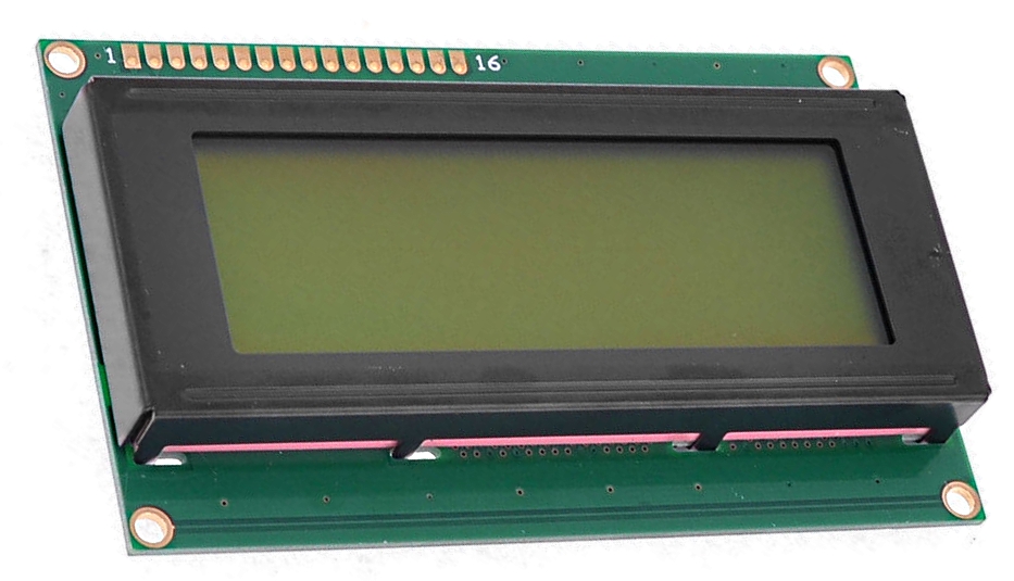
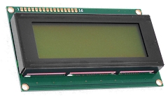
LCD Display - this
is the recommended option |
|
 |
Real Time Clock -
this is the recommended option |
| |
Location dependent
on internal / external mounting choice -
see notes |
|
|
Seq. No. |
Description / notes |
Photo |
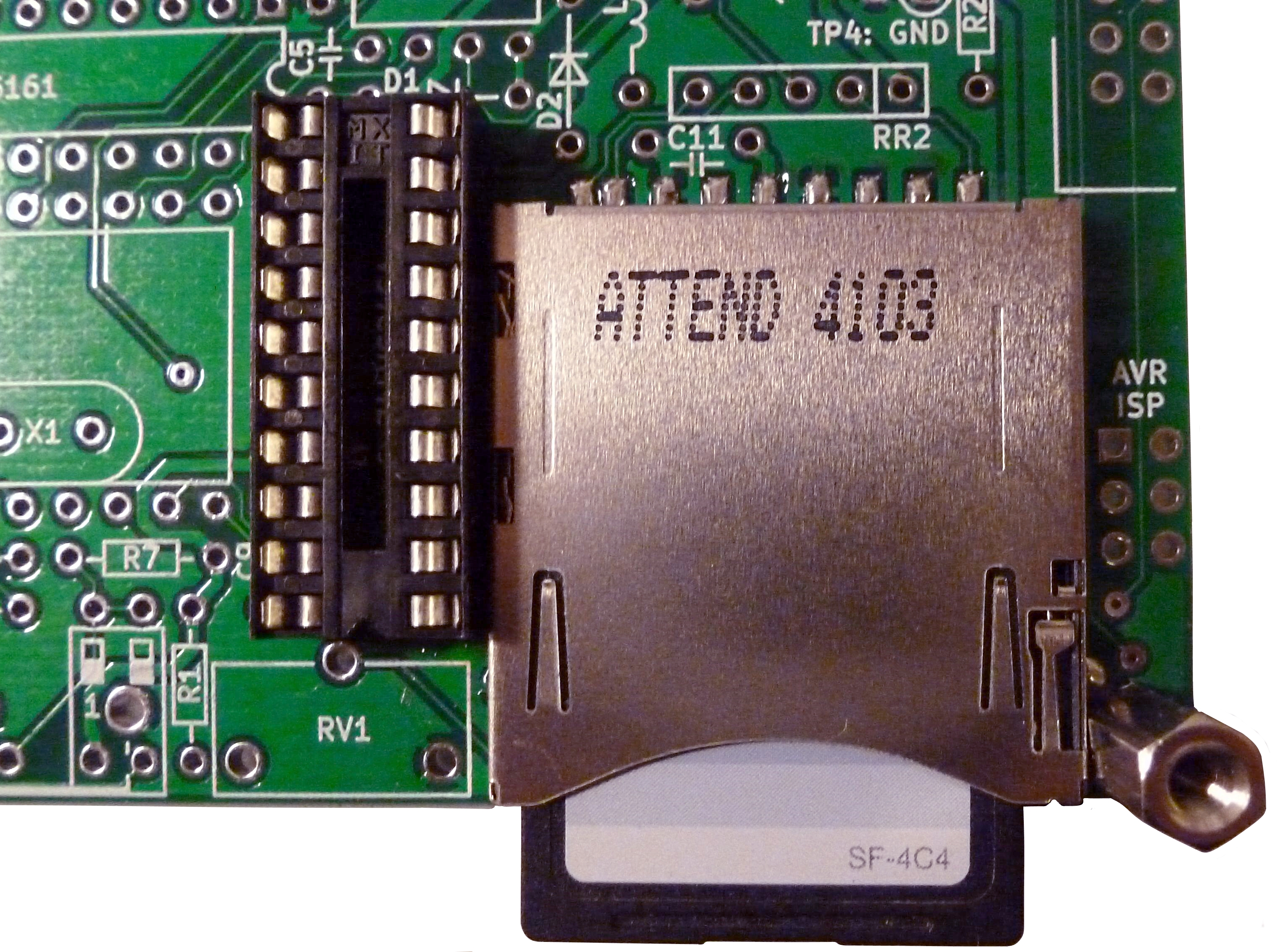
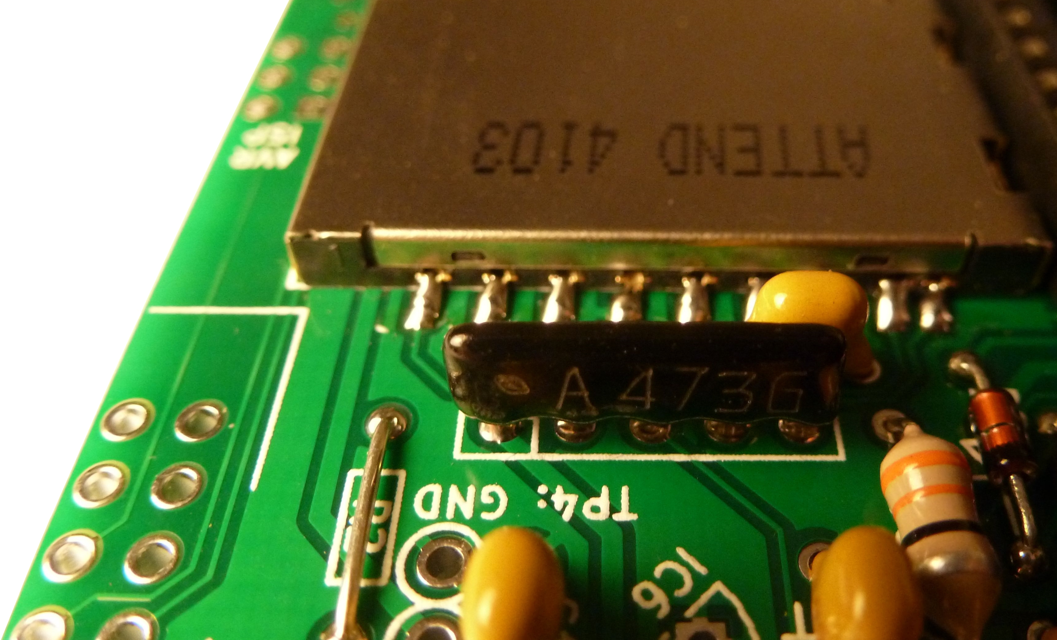
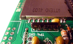
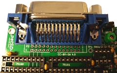
| 1 |
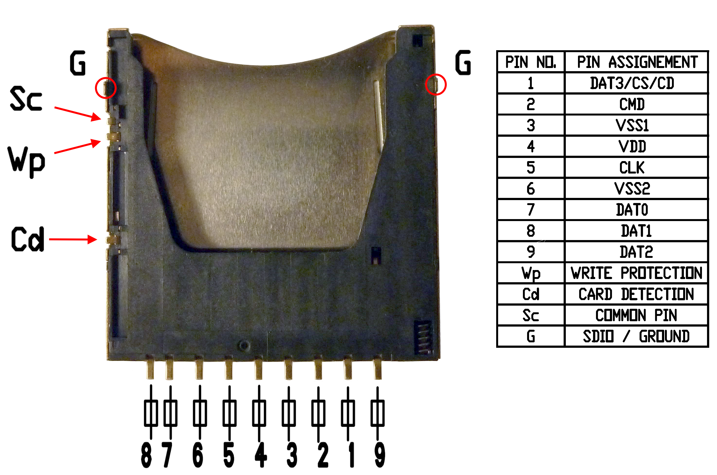
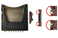
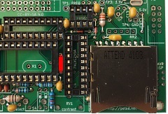
Details for the SD Card slot - model : Attend
104H-TDA0-R As you can see, the contacts,
particularly those for, Signal Common
(Sc), Write Protect (Wp) and
Card Detect (Cd) are a bit on the small
side, with Sc and Wp very close together ! |
 |
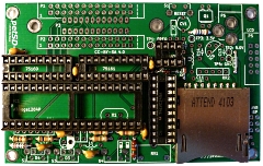
| 1 |
Mount the SD card slot
For maximum stability, the slot should be placed
with the two locating pins near the front of the
slot set into the holes provided.
The slot should be
positioned as far to the left as the solder pad
positions will allow to ensure that there is enough
room for the spacer bolt to the right.
Here, an unsoldered DIP-20
socket has been been placed in the IC4 position to
ensure that there is acceptable clearance on both
sides. |
 |
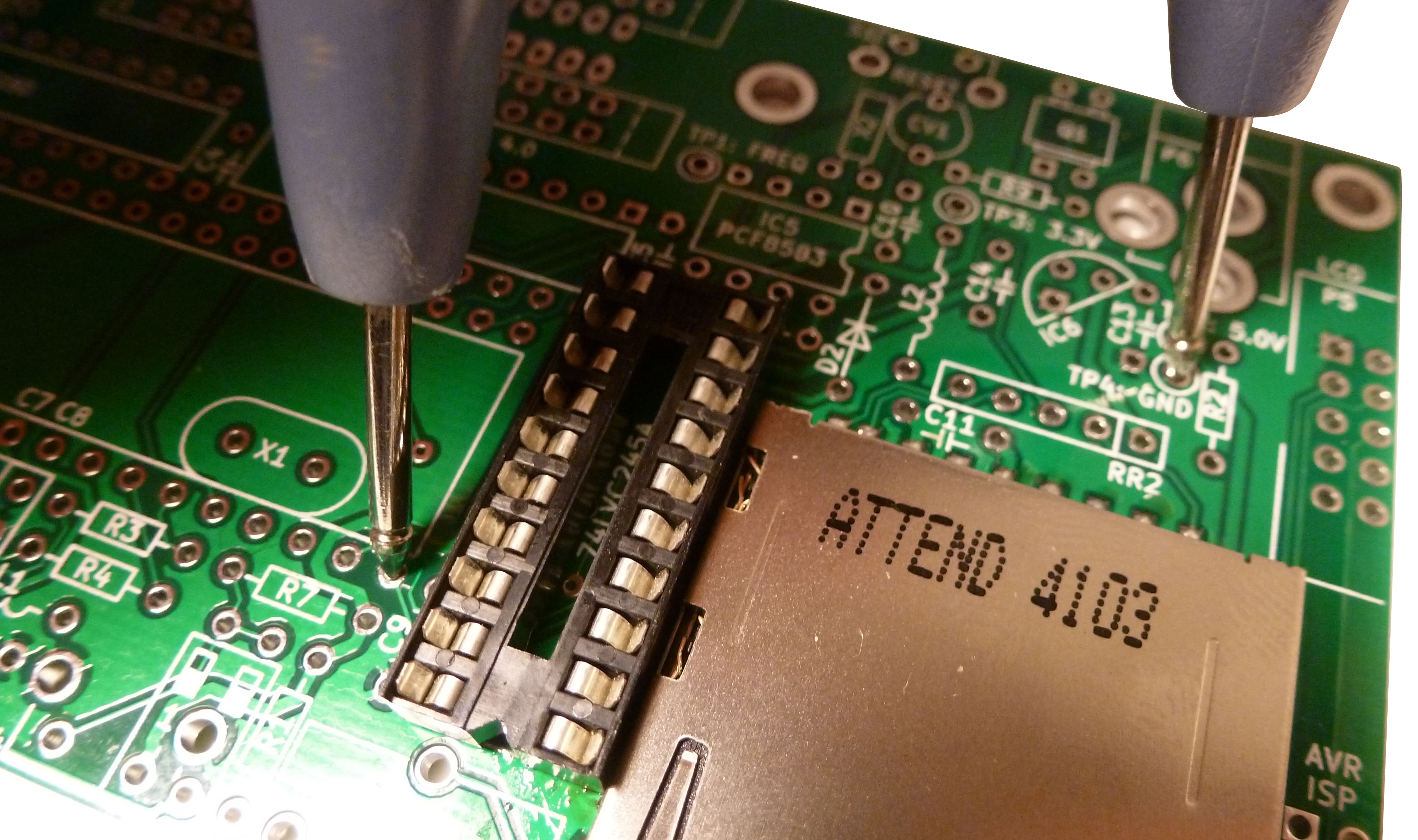
| 1 |
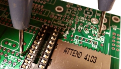
Apply some solder onto the
three pads on the left side of the slot first, then
place the slot, clean your soldering iron tip heat
the leads only without applying extra solder.
The solder that you applied
before should melt and give a good connection
without shorts. The remaining terminals at the rear
of the SD card slot should now be soldered to the
PCB.
Verify
your work with a continuity tester and an SD card |
 |
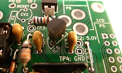
| 1 |
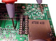
Set the card's Write Protect
(WP) switch to the LOCKed position (writes disabled)
- insert the card - measure between Signal
Common and pin
20 of the MCU (IC1) (Write Protect) as shown
Provided that your continuity tester comes with a
buzzer:
If the card is completely inserted with write
protect on, there will be silence. If it is removed
half the way, it will beep. If this is not the case,
either the Wp, the common connection
Sc or both are
bad. |
 |
| 1 |
Verify the Card Detect switch
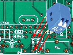
Measure between ground and pin 19 of the MCU as
shown
If the card is pushed in completely, it will
beep, if it is removed (half way), there will be
silence.
Make sure, both switches are working NOW!
It will be almost impossible to fix them later!
|
 |
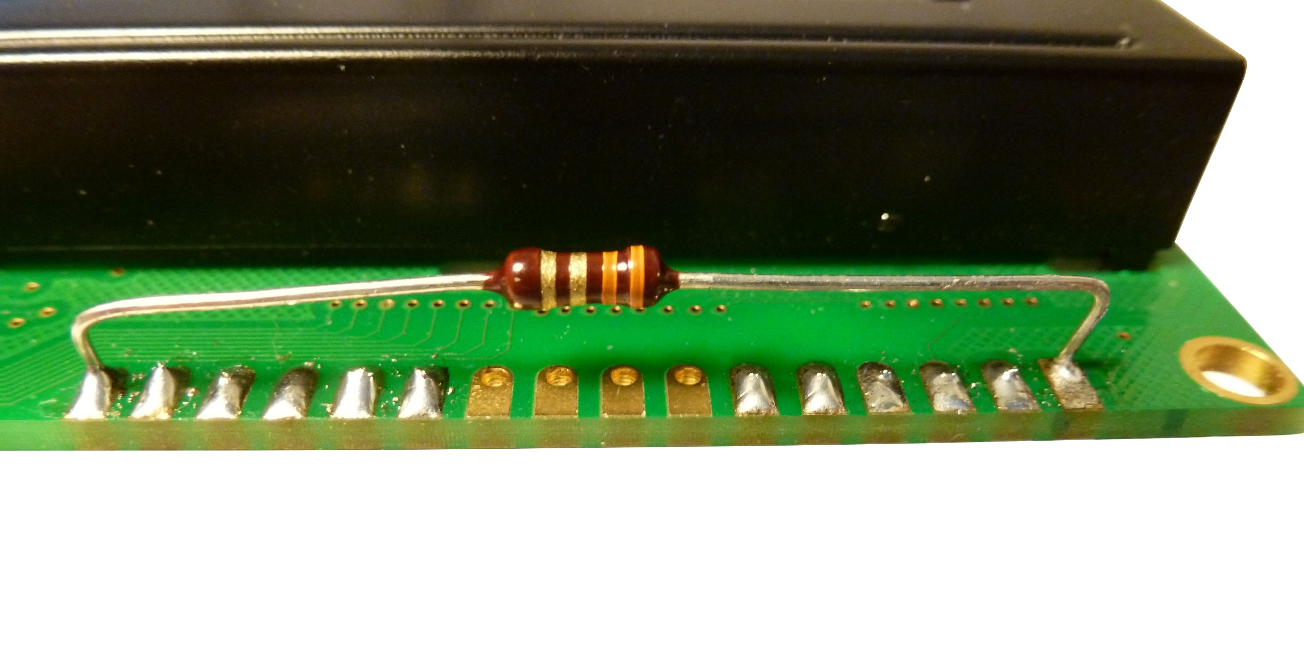
| - |
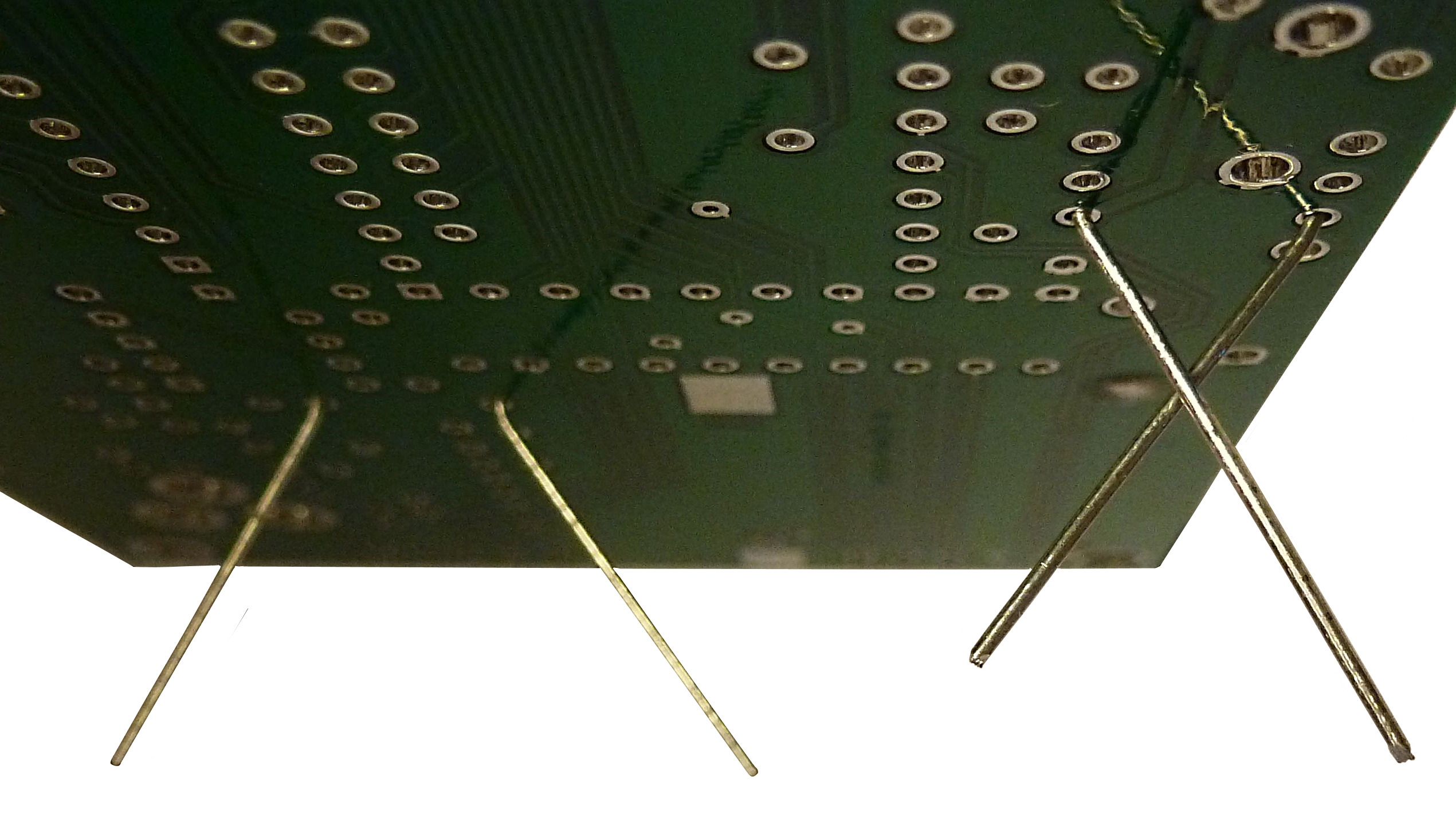
***
TIP *** Bending the
component legs
This
photo shows how the component legs should be bent
prior to soldering. The component on the left has
its legs bent outwards and can easily product shorts
to adjacent components.
The one
on the right has its legs bent inwards and is the
safer method to follow. |
 |
| 2 |
|
|
|
(Required for LCD only) |
 |
| 3 |
|
|
|
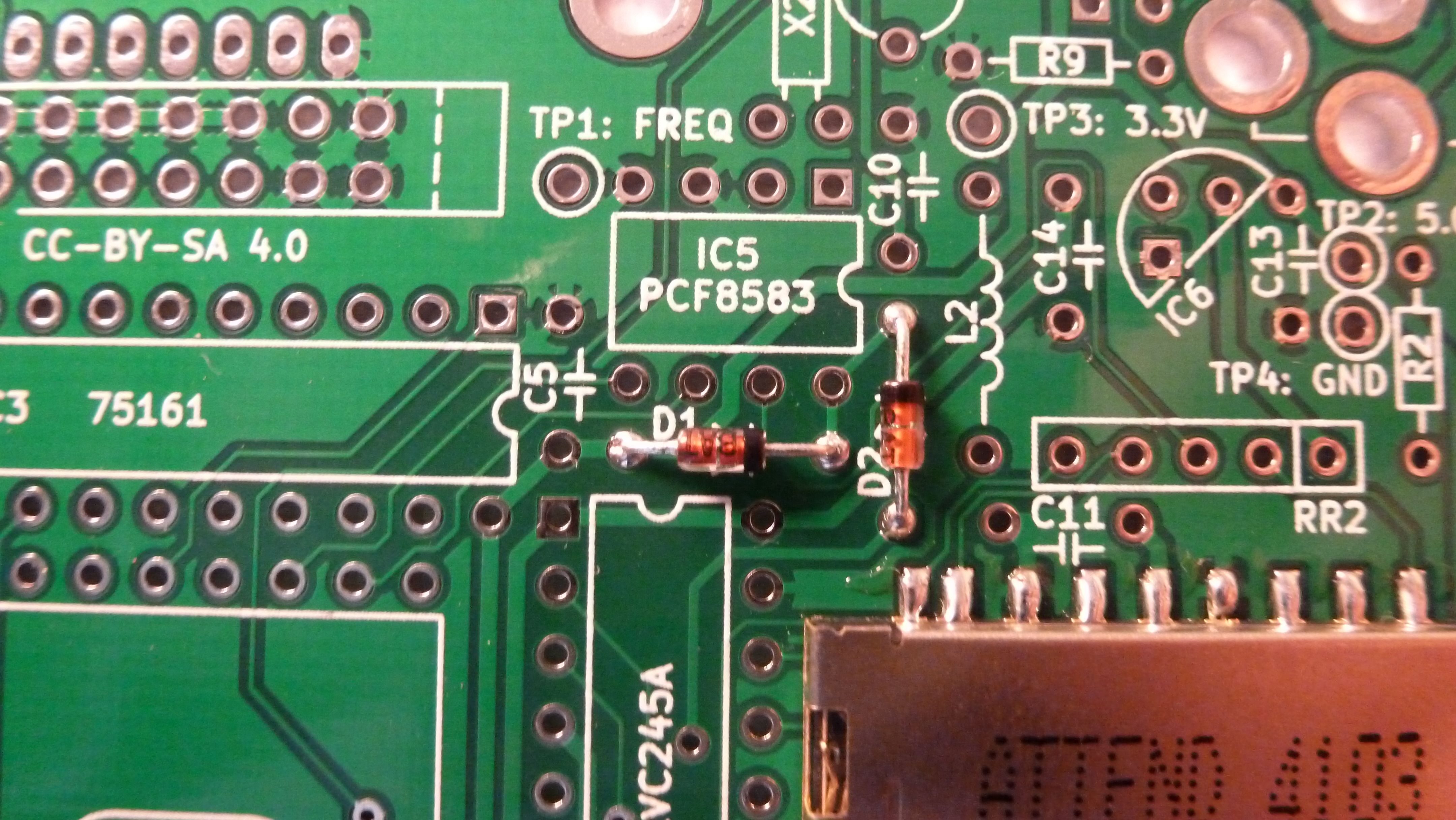
| D1 & D2 |
Schottky diode, DO35, p/n
BAT42 |
Check the orientation of the diode to ensure
correct polarity
(Required for RTC only) |
 |
| 4 |
|
 |
| 5 |
|
 |
| 6 |
|
 |
| 7 |
|
 |
| 8 |
|
|
|
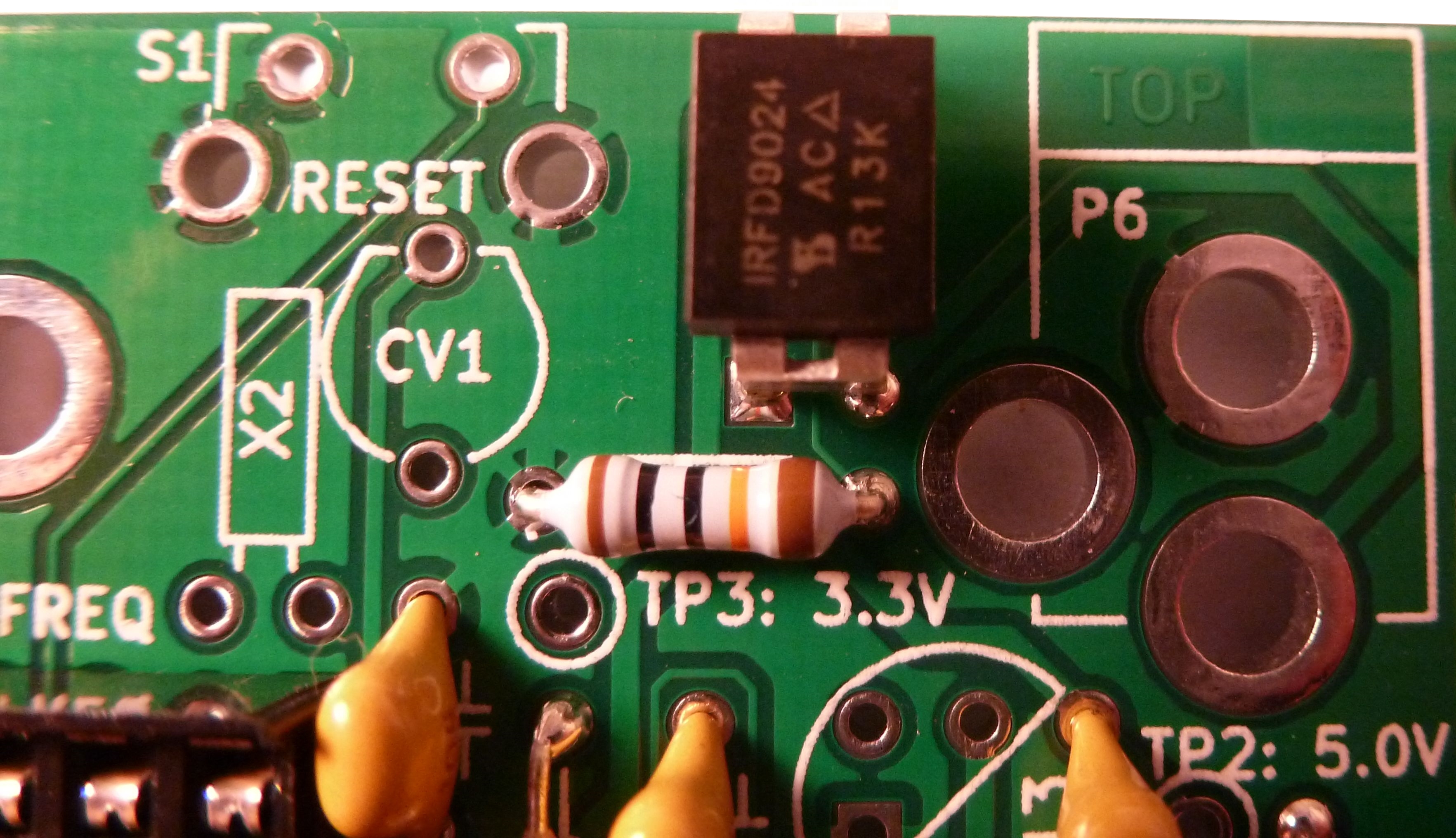
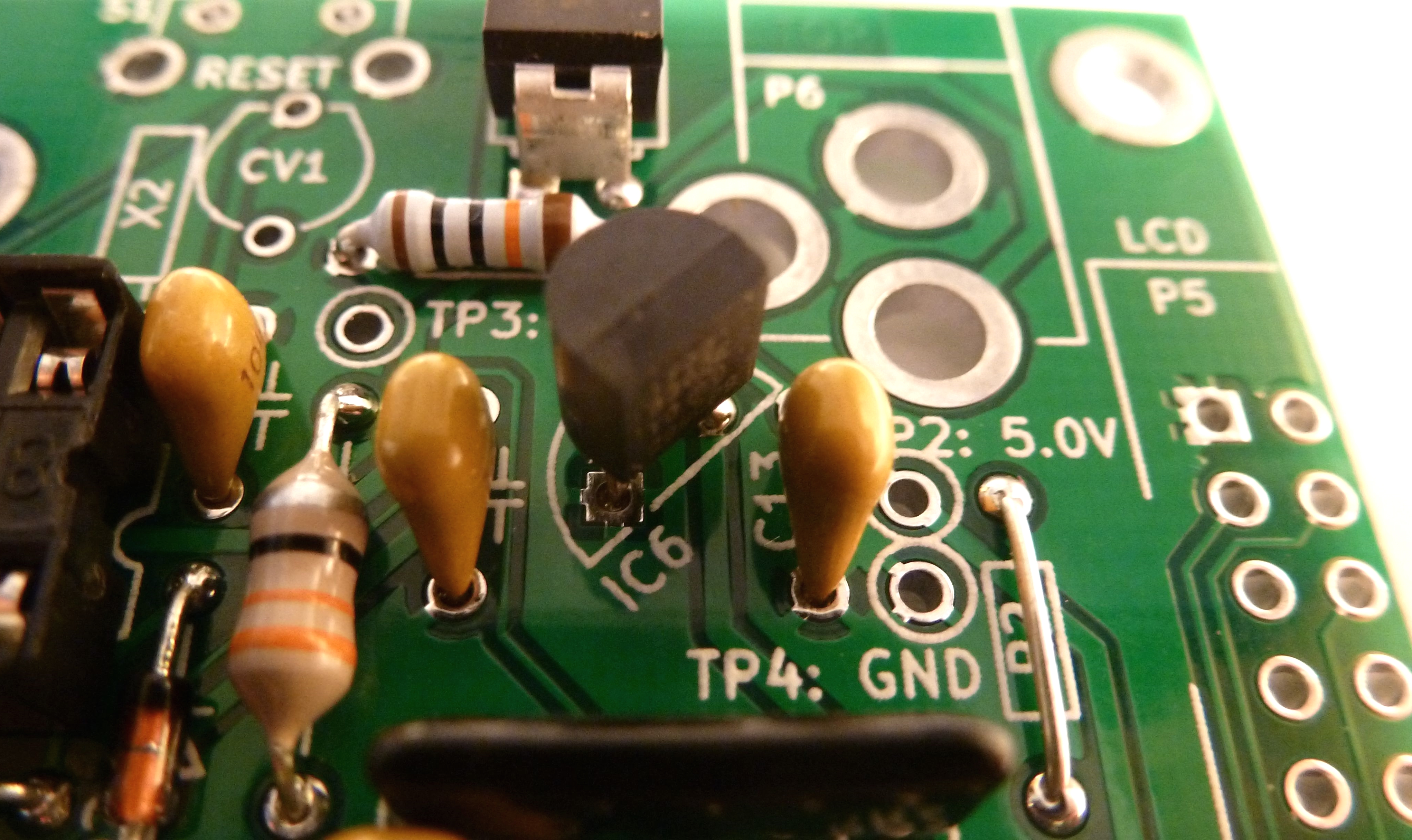
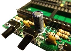
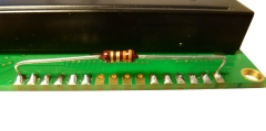
R2 is the resistor for
the LCD backlight, its value depends on the
actual display used. Placing the resistor on the
display itself, rather than on the PCB, will
make it easier to replace it should it be
necessary to change the type of the display. In
that case, a wire link should be put in the R2
position on the PCB (See "e"
below).
(Required for LCD only) |
 |
| 9 |
|
 |
| 10 |
|
 |
| 10a |
The external oscillator (X1) for
the MCU was intended to be installed inside the MCU
socket, however, on the Version 1.0 PCB, there is
not enough clearance.
The "work-around" is to
fit the oscillator to the underside of the PCB, it
is easier to install the oscillator BEFORE fitting
the socket.
This has no practical impact for
units fitted with the RTC since the coin cell holder
is also mounted on the underside of the PCB. |
 |
| 11 |
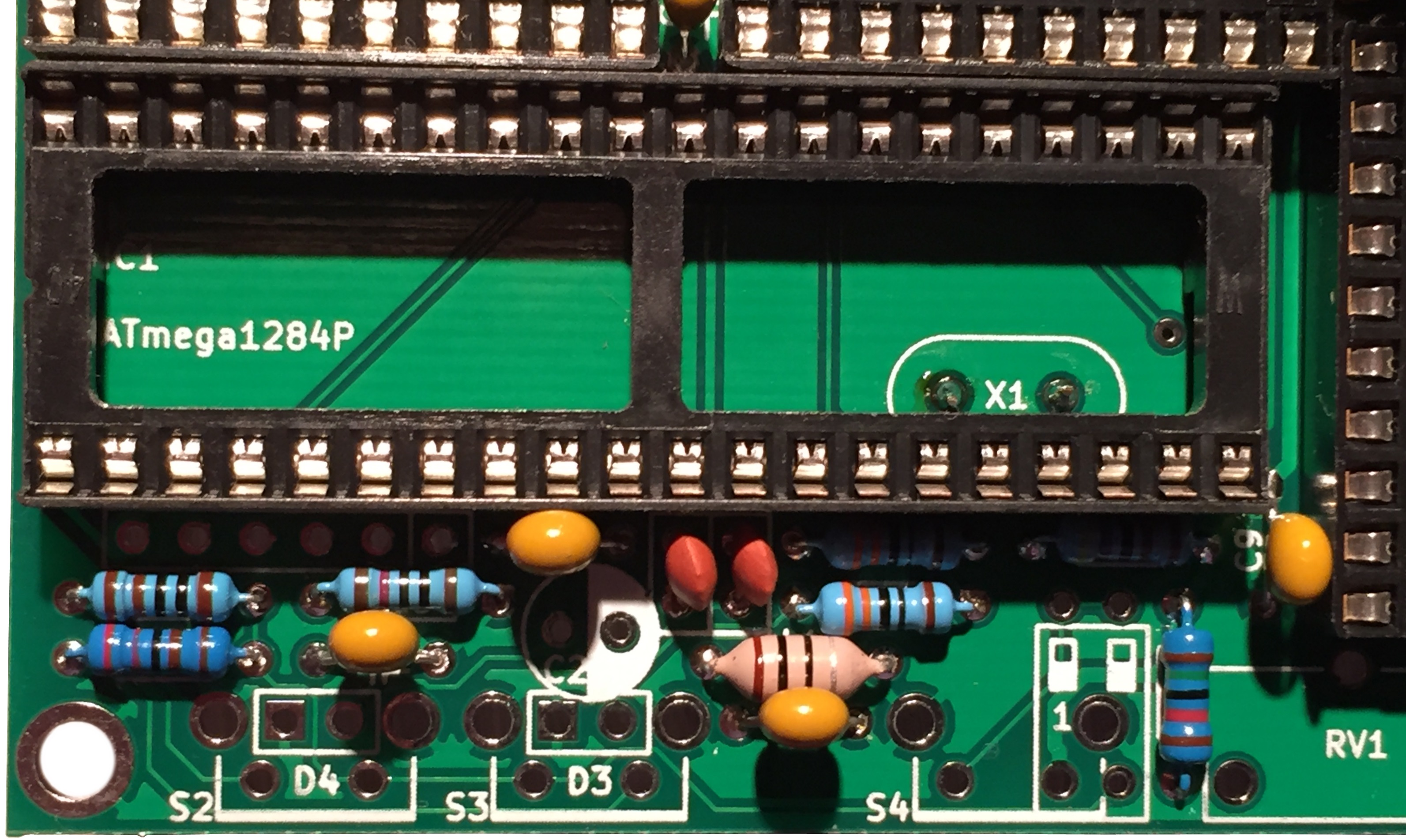
Install the sockets for IC1, IC2,
IC3 and IC4 |
 |
|
|
Install the socket for IC5
(Required for the RTC only) |
| 11 |
Ensure that the notch in
the sockets is placed at the mark on the PCB as
shown in this example |
 |
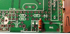
| 11a |
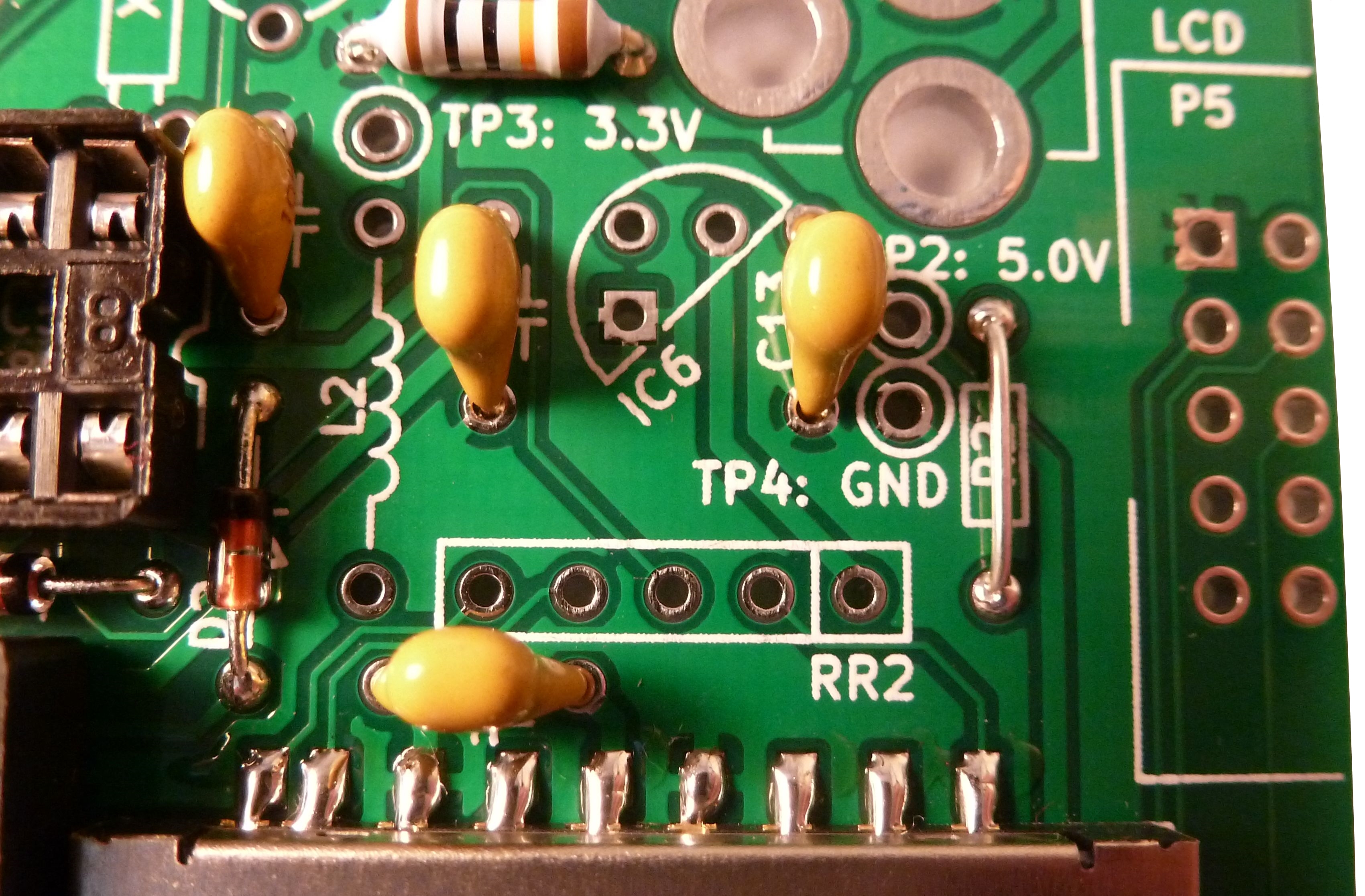
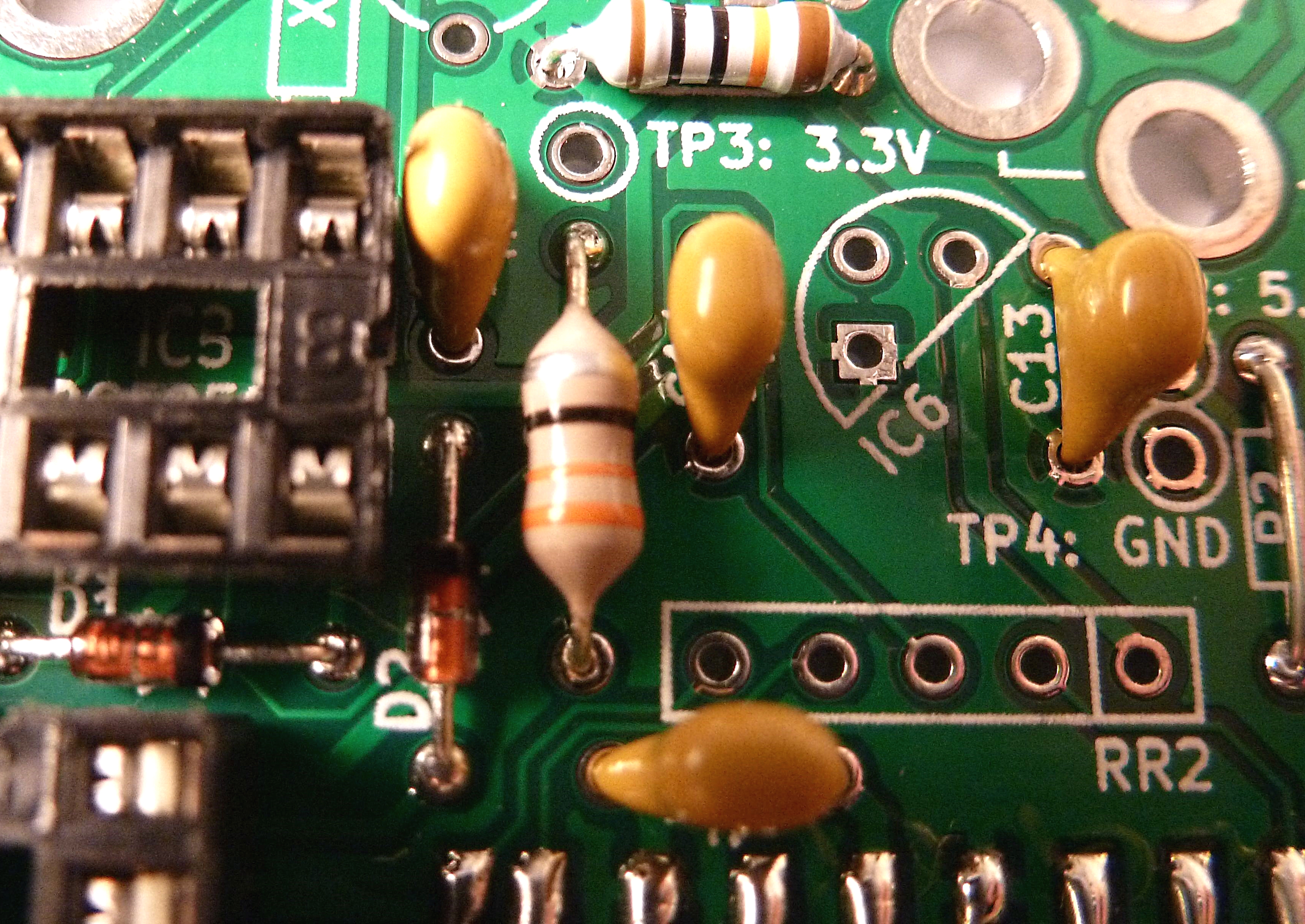
For PCB revision V1.1 and later, R10 is no
longer an optional component and should be installed between the
sockets for IC1 and IC4 as shown by the red mark-up
in this photo.
Note: PCB Version
1.1 is missing the component label for R10. |
 |
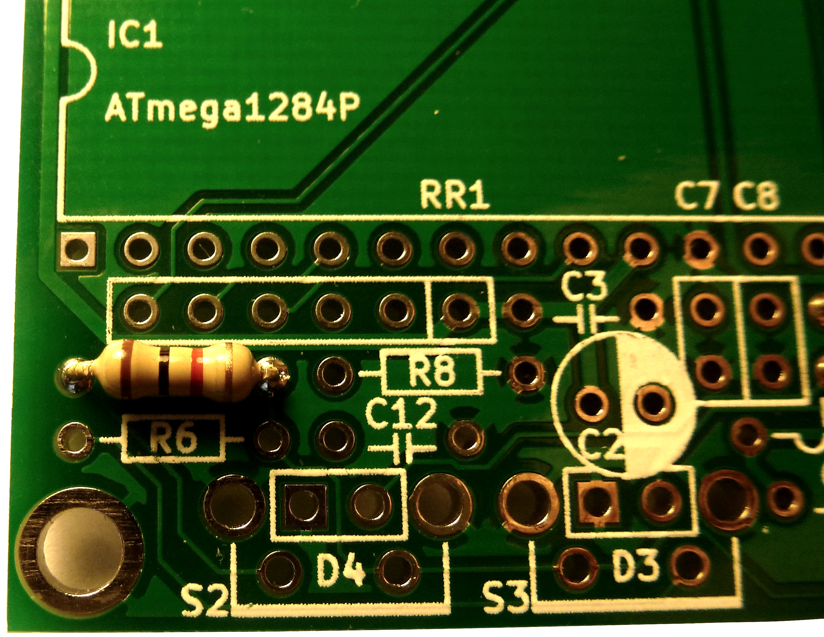
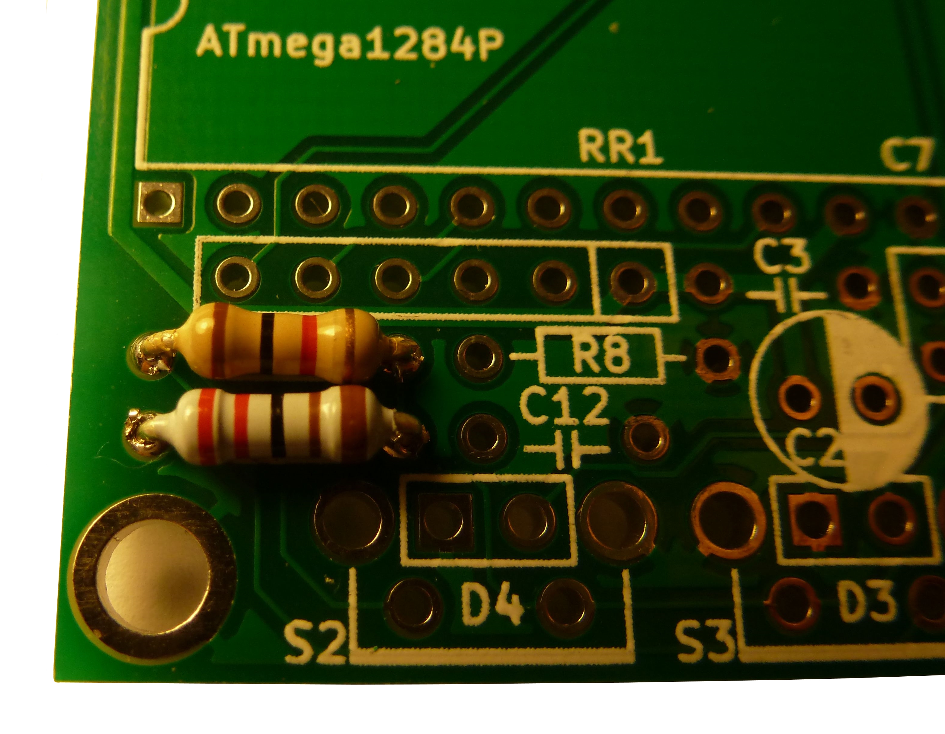
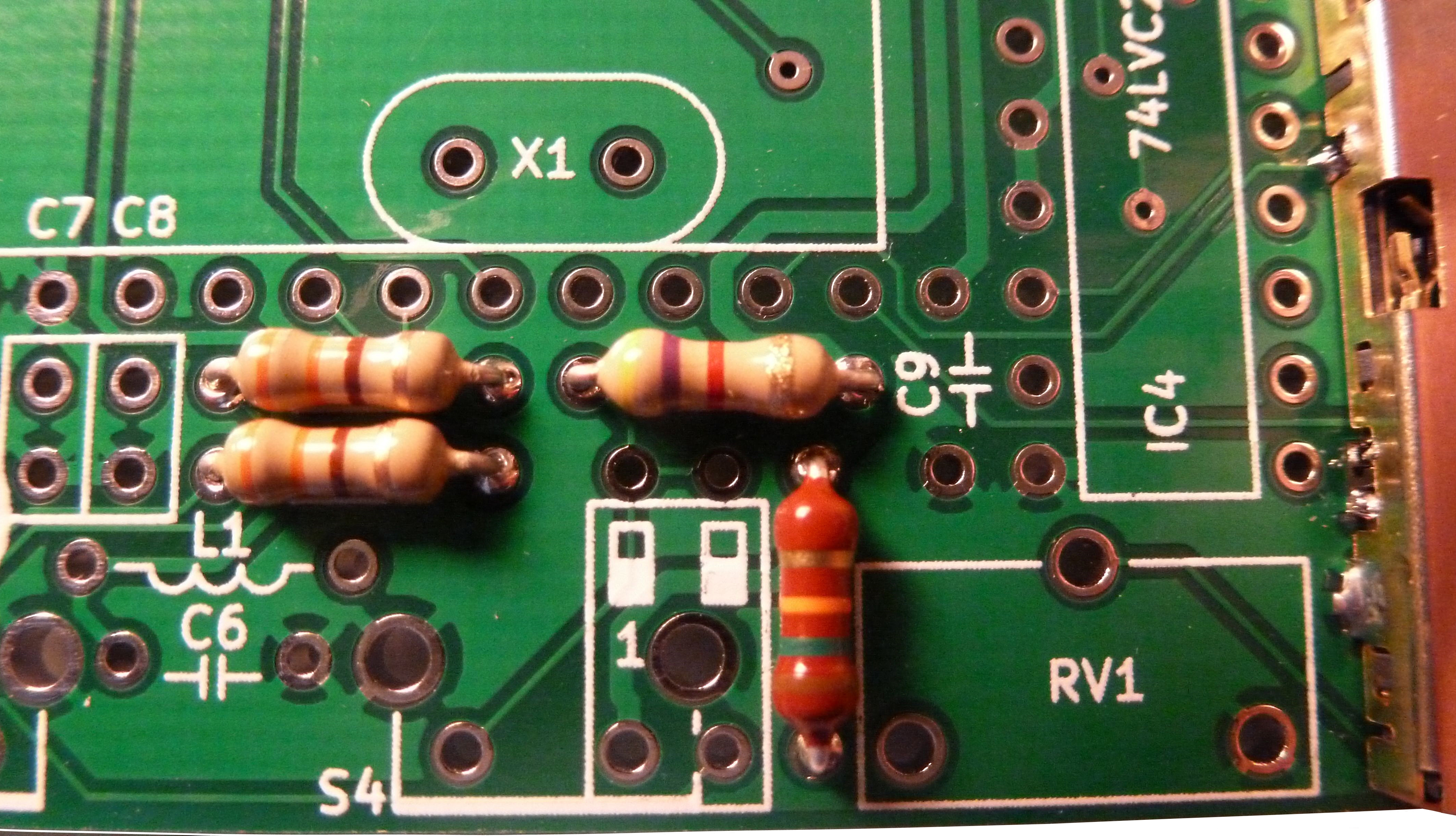
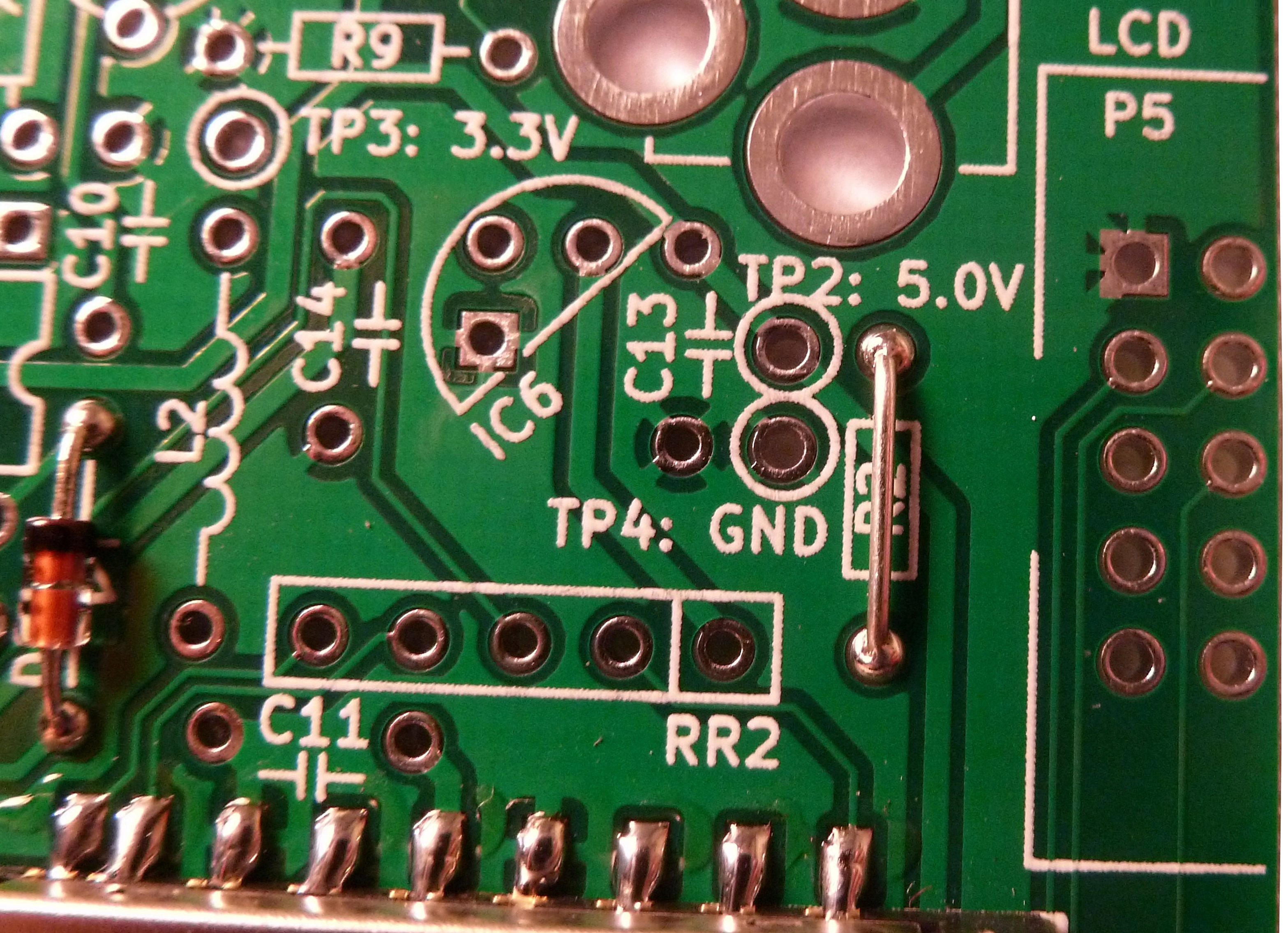
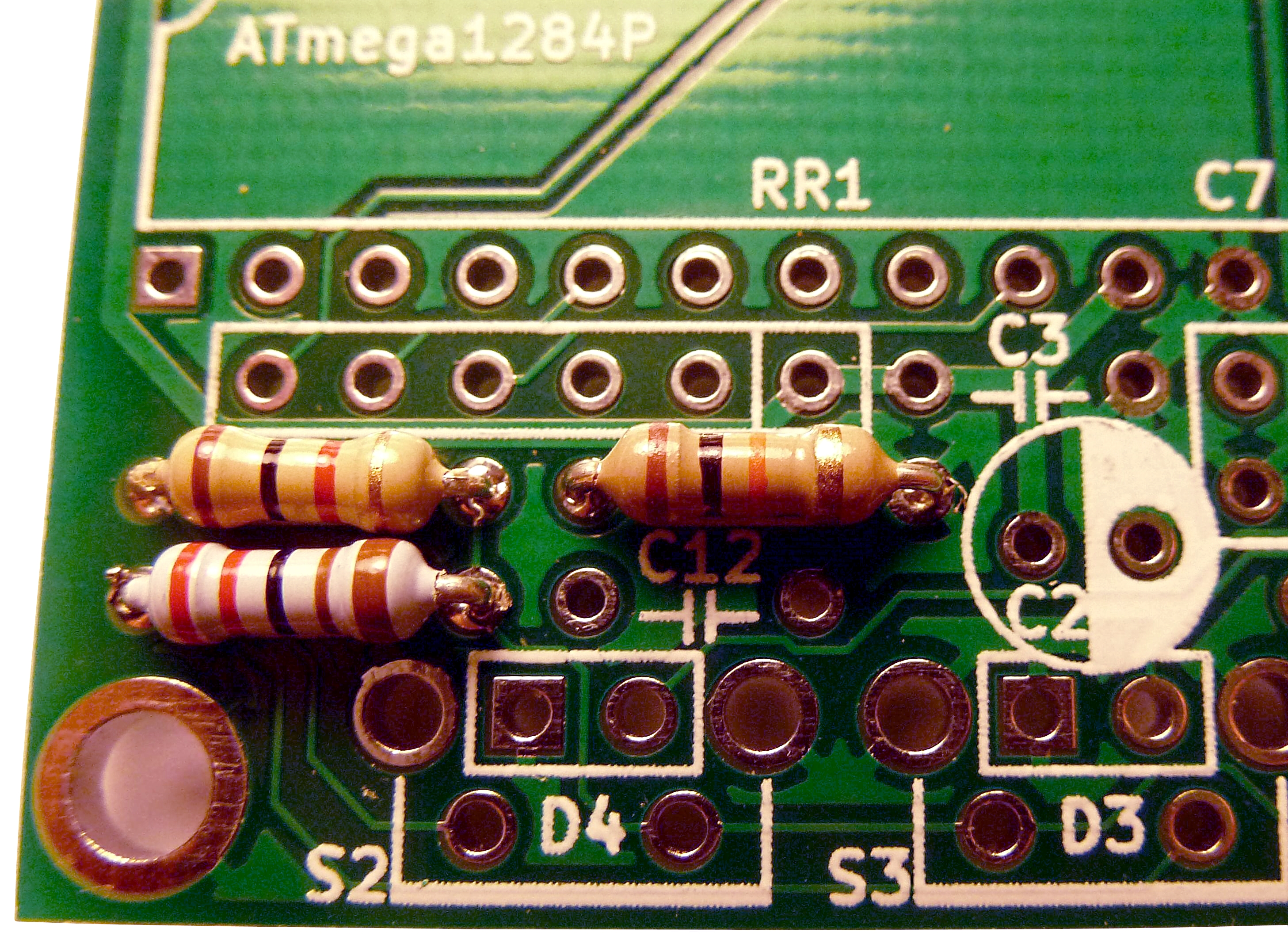
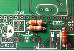
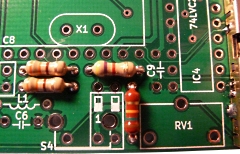
| 12 |
|
C1, C3, C4 |
100nF |
|
C5, C6, C9 |
100nF |
|
C12 |
100nF
DELETED - DO
NOT INSTALL |
Manufacturing tolerances mean that some of the
ceramic capacitors in the kit can be somewhat
thicker than others. C4 and C5 are fitted
between IC sockets 2, 3 and 5, fit these first
so that you can choose the most suitable
capacitors for these locations.
|
 |
| 12a |
The capacitors for the X1 oscillator are the
orange ones just next to the MCU socket.
|
 |
| 13 |
|
|
|
|
 |
| 14 |
|
 |
| 15 |
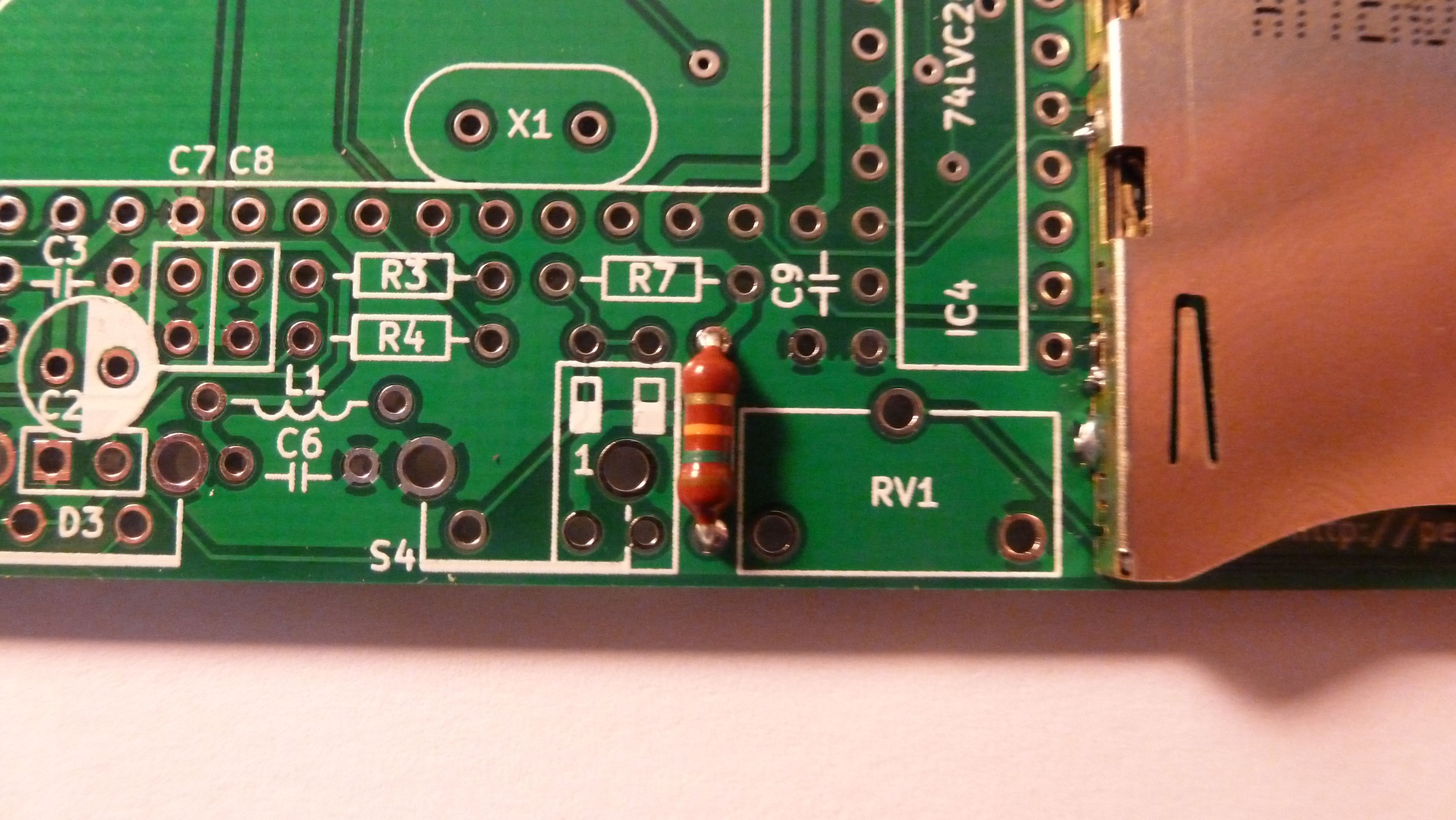
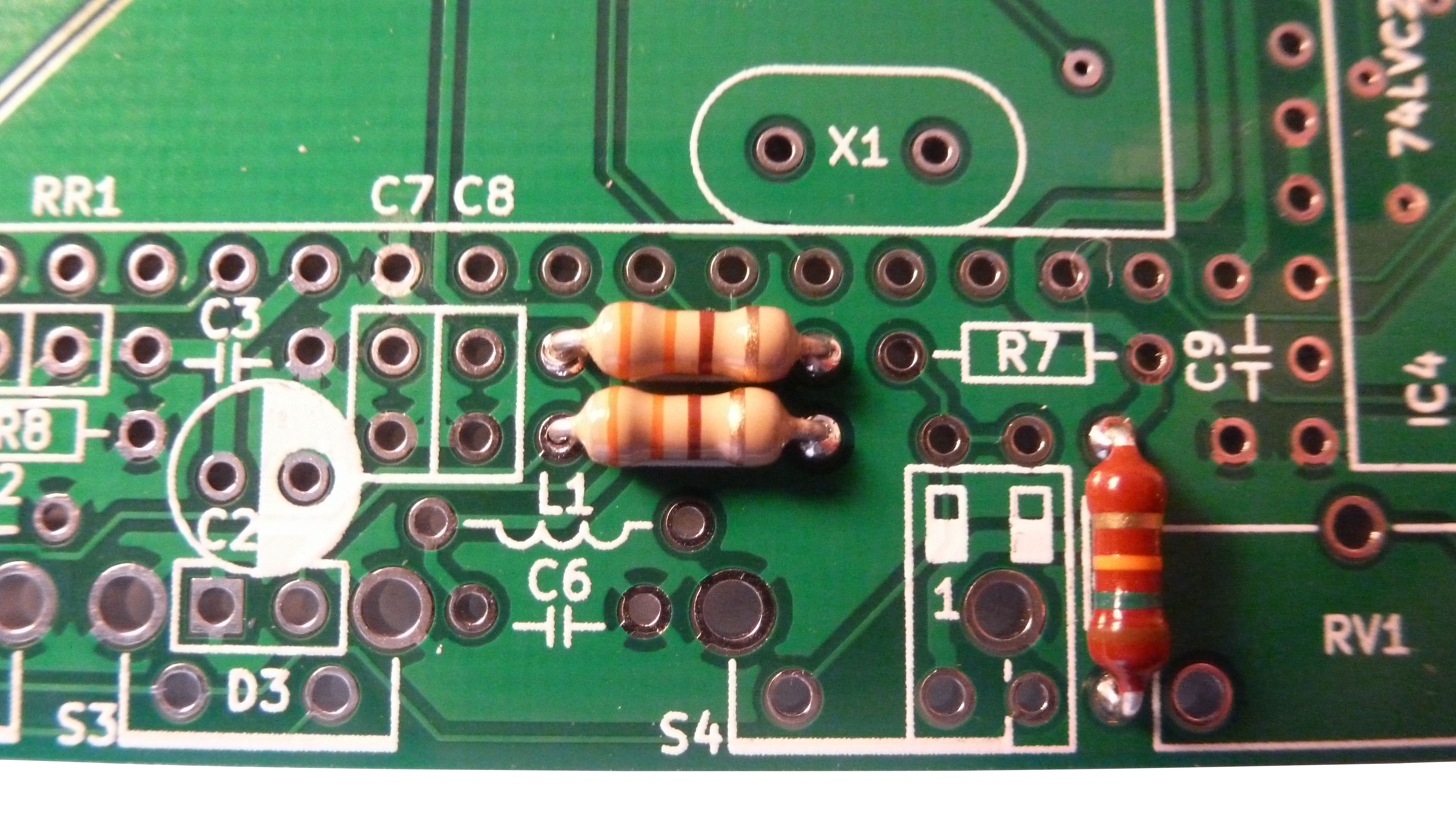
| L1 |
10 uH, 200 mA, diameter <= 4 mm |
|
 |
| 16 |
| L2 |
33 uH, 200 mA, diameter <= 4 mm |
|
 |
| 17 |
Take care to position the
transistor correctly, as shown
|
 |
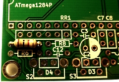
| 18 |
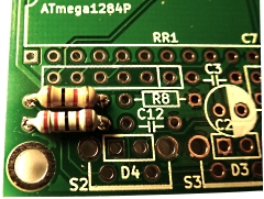
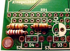
| RR1 |
5 x 10k Resistor Package |
Ensure that the "dot" on the
package is aligned with the index mark on the
PCB (the square box at one end of the RR1
stencil)
|
 |
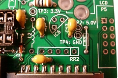
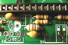
| 19 |
| RR2 |
4 x 47k Resistor Package |
Ensure that the "dot" on the package
is aligned with the index mark on the PCB (the
square box at one end of the RR1 stencil) |
 |
| 20 |
|
 |
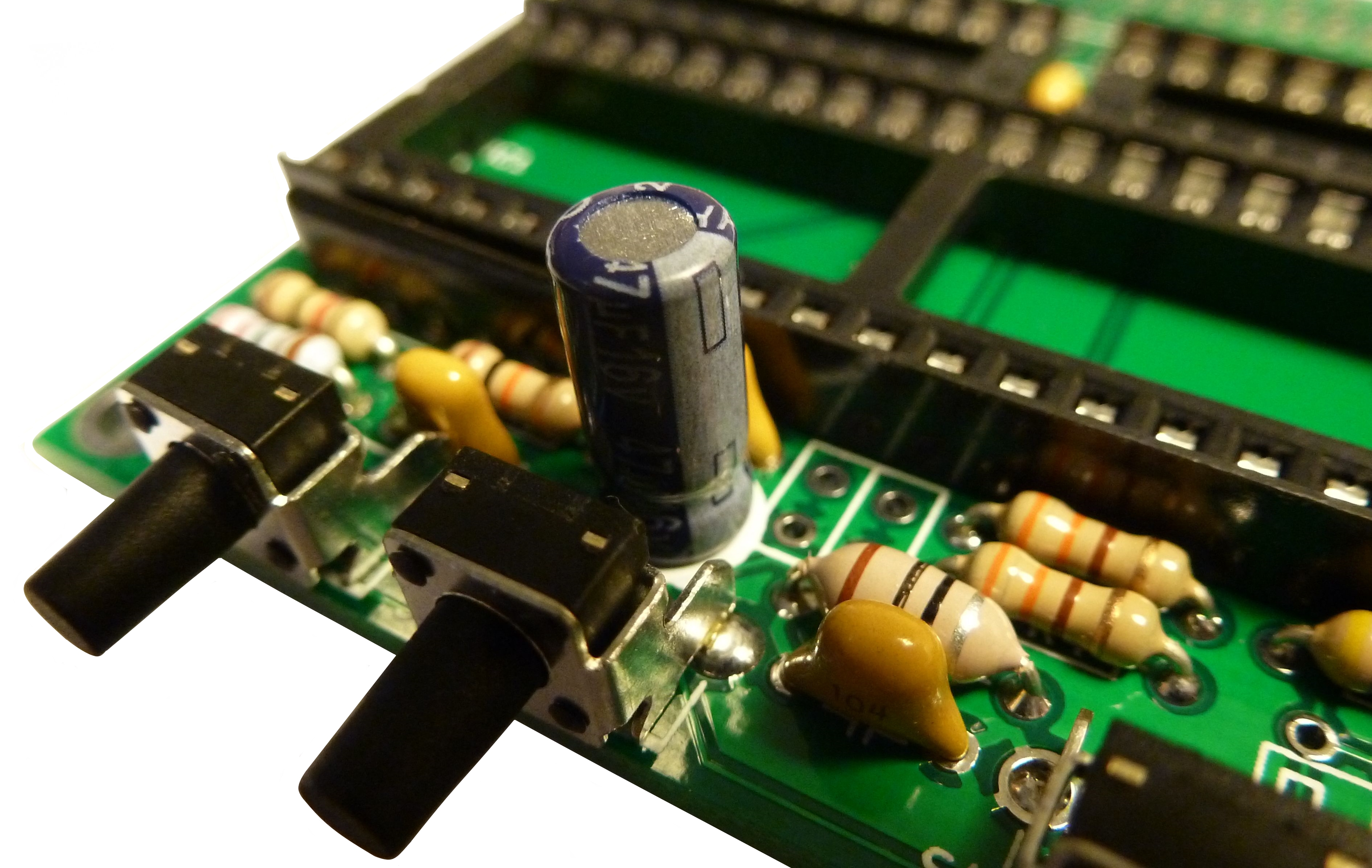
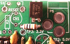
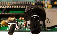
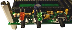
| 21 |
|
S1 |
APEM PHAP3305B (Reset) |
|
 |
|
S2 |
APEM
PHAP3305B |
("Previous") |
|
S3 |
APEM
PHAP3305B |
("Next") |
|
S4 |
APEM
PHAP3305B |
("Select") |
The
default (preferred) location for these switches is
on the PCB, if petSD+ is to be mounted internally to
the PET, these switches and LCD display can be
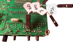
mounted remotely. |
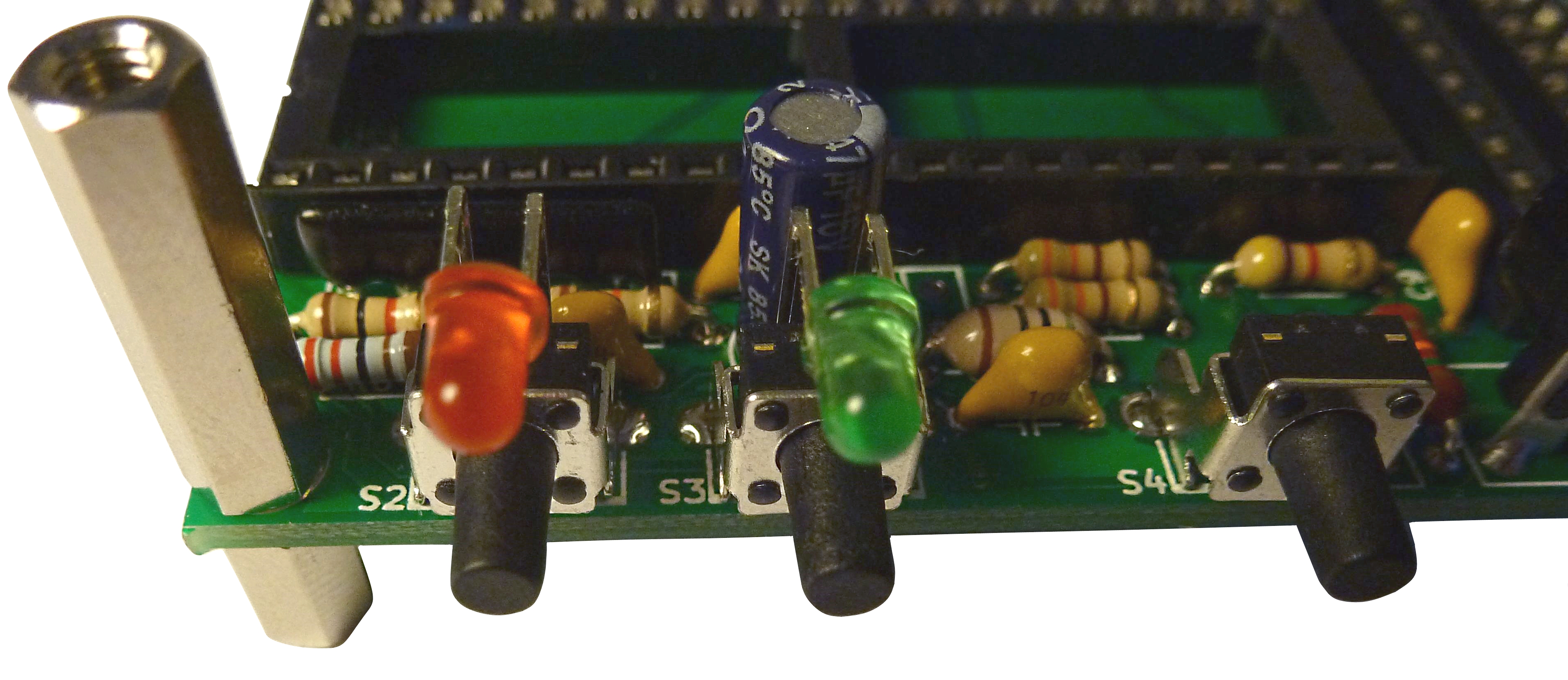
| 22 |
|
|
|
| P5 |
10 Pin box header |
(LCD connector) |
Ensure header is located with
keyway facing inwards
(Required for LCD only)
|
 |
| 23 |
|
P6 |
Barrel jack,
6.3x2.1mm |
***
TIP *** Positioning the
power socket
It is very easy to end up with the power socket
off-centre, this can look very ugly but securing
the socket with a small amount of glue will
allow it to be accurately placed before
soldering .
|
 |
| 24 |
Ensure
that the polarity is correct |
 |
| 25 |
|
|
|
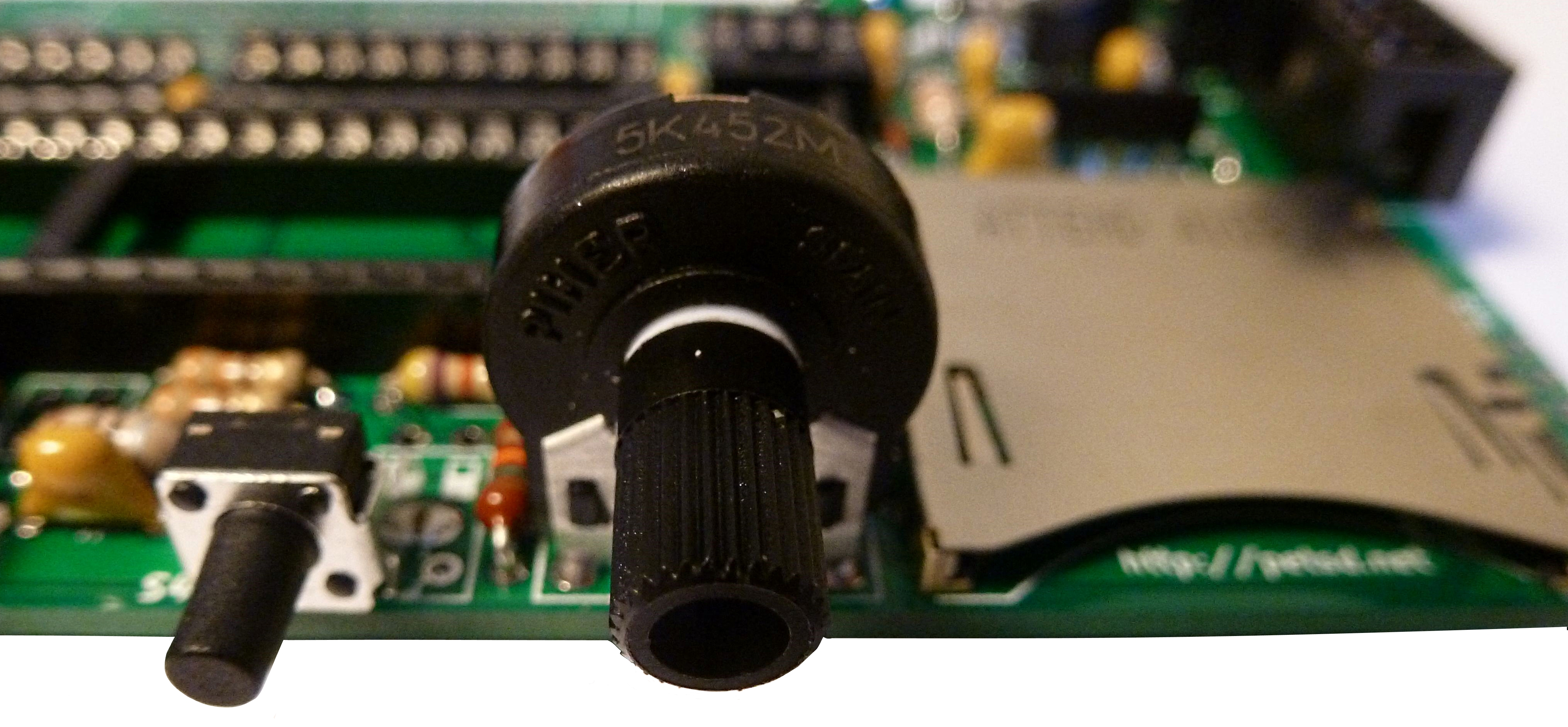
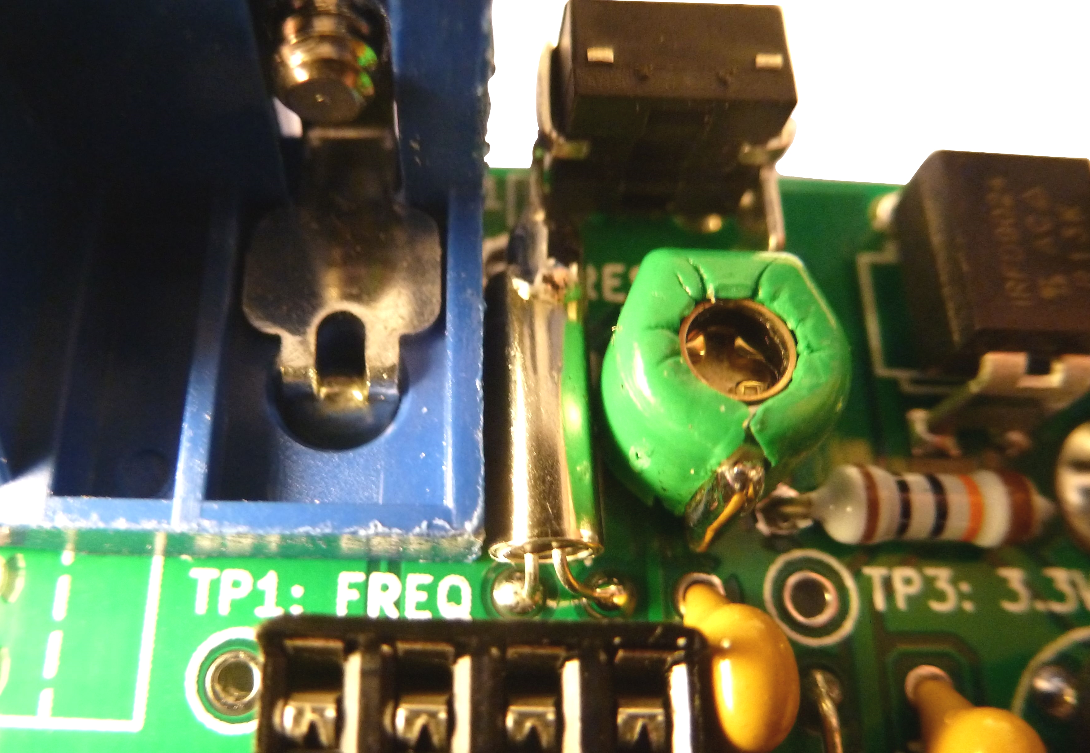
|
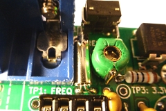
CV1 |
5-25pF
Variable Capacitor |
|
 |
| 26 |
|
|
|
|
 |
| 27 |
| |
|
|
|
|
|
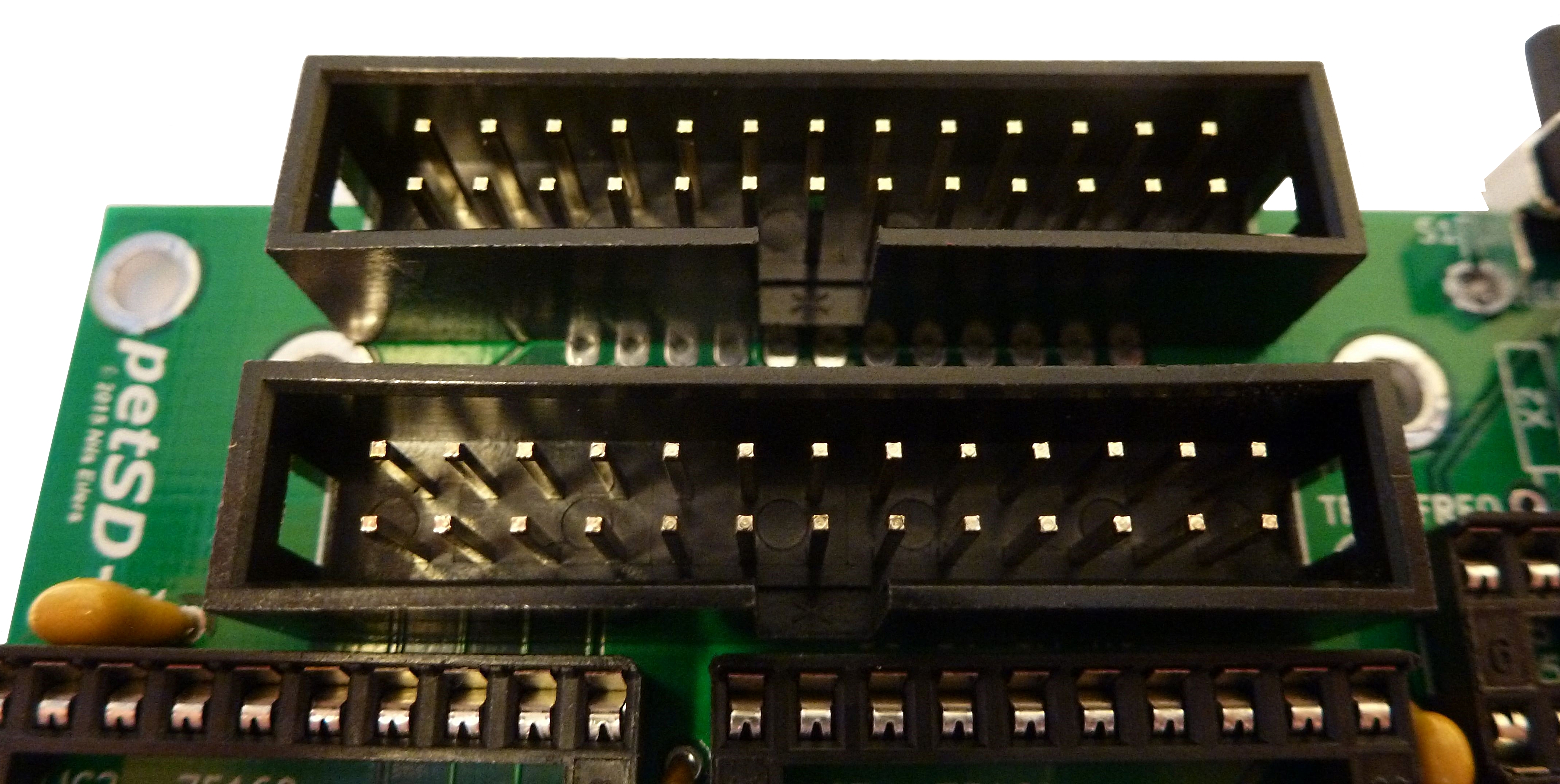
P1, P2 |
2 x 12 or 2 x 13 Pin Headers (for
IEEE-488) |
|
Ensure headers are located with
keyway facing inwards |
|
OR |
|
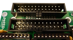 |
|
|
| |
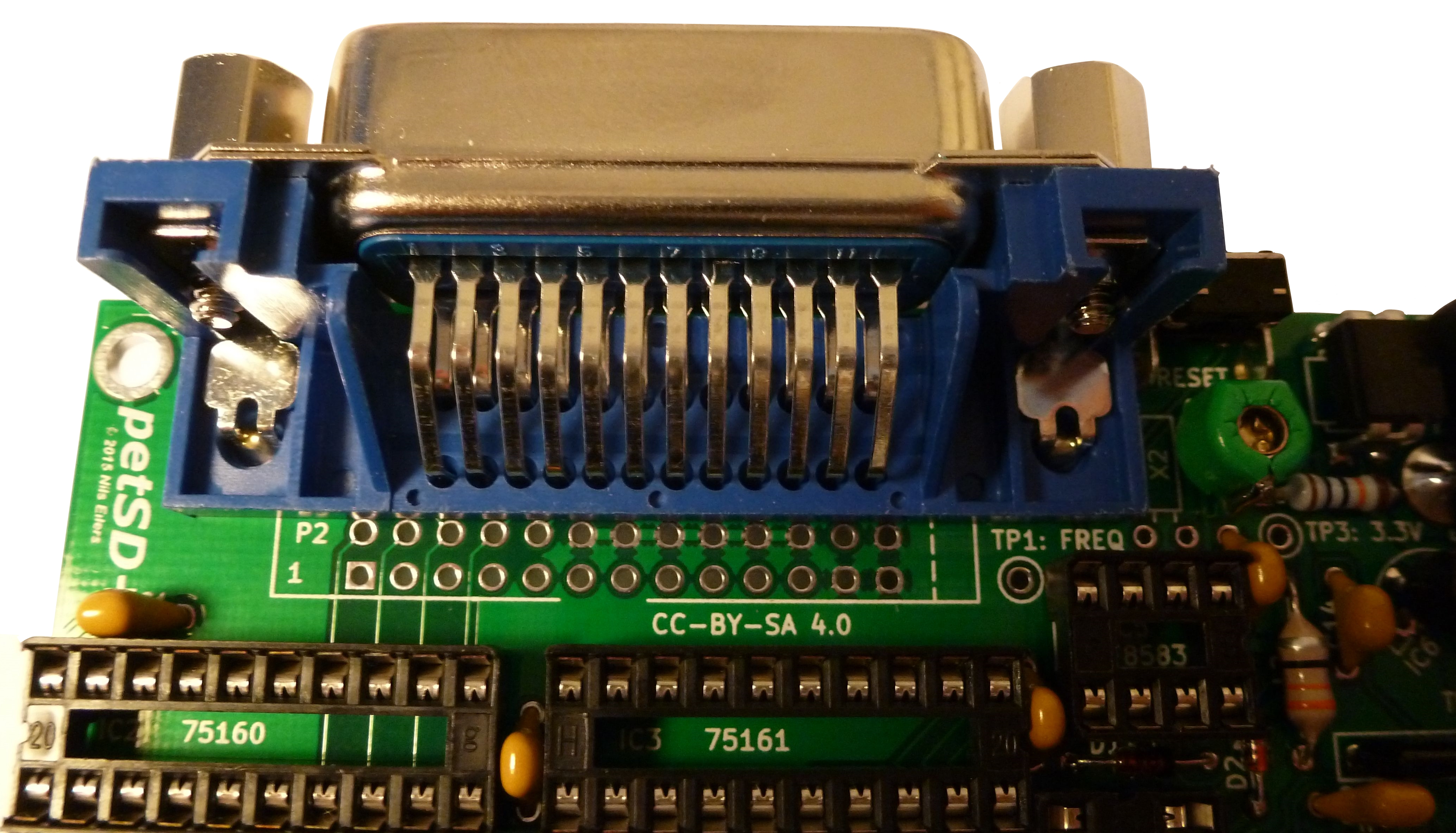
|
|
P3 |
IEEE-488
Connector |
| |
|
| The PCB has header
positions for either a
proper IEEE-488 connector or
2 x dual row pin headers which can be
used for in/out IEEE-488 ribbon cable
connections. Note : The PCB has
space for only 1 of these options |
|
 |
| 28 |
|
|
|
|
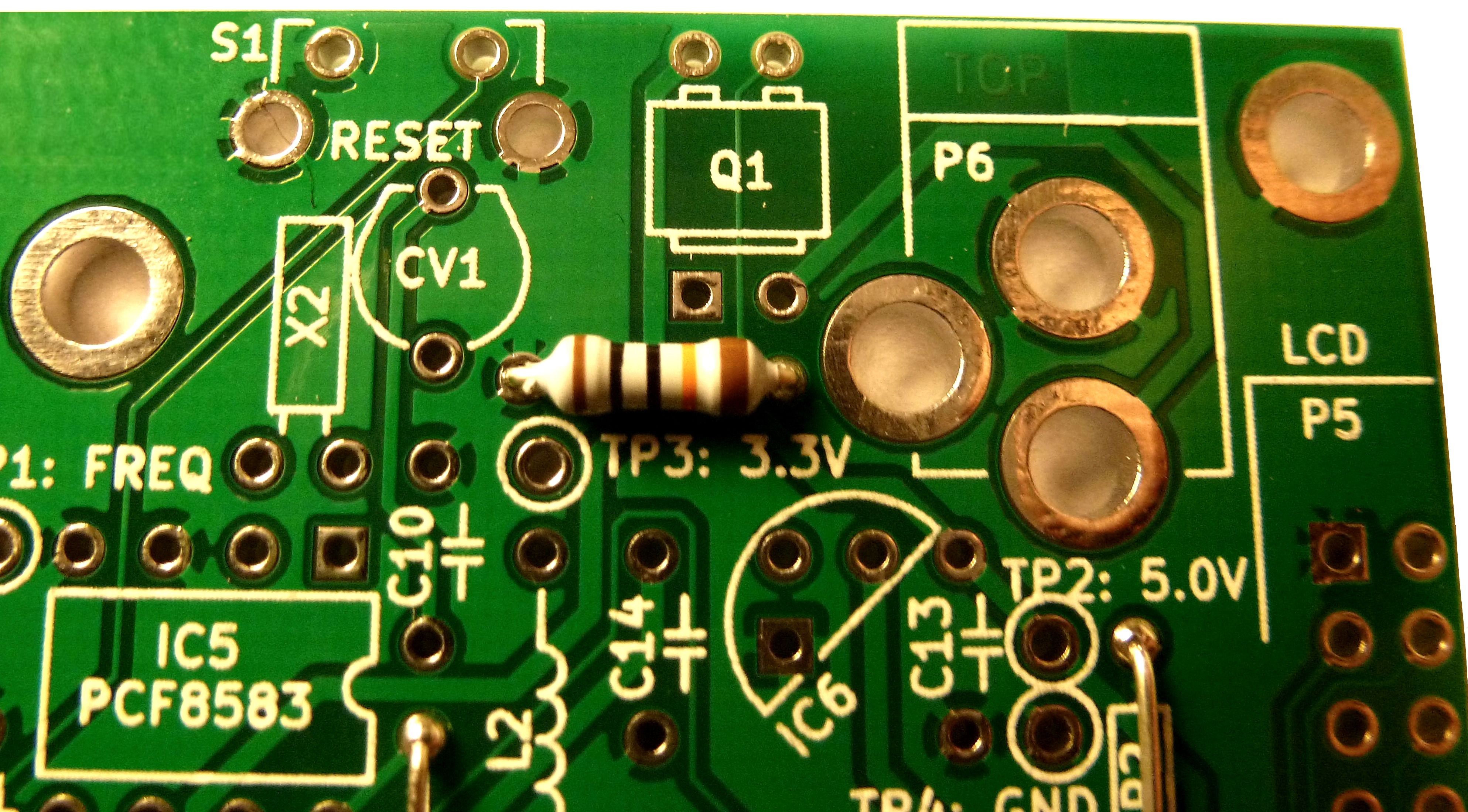
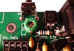
X2 |
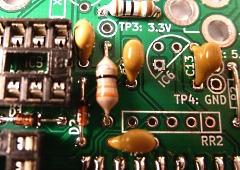
32.768 kHz oscillator for RTC |
Take care
to not short the crystal's case with one of the two
connections, make sure that there is some clearance
between the can and the PCB. Verify that there are
no shorts with the continuity tester. To ground the
case, apply some extra solder at the top end of the
can and bridge between the can and the reset switch
ground connection. |
 |
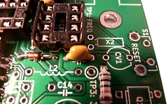
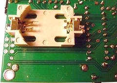
| 29 |
|
|
|
|
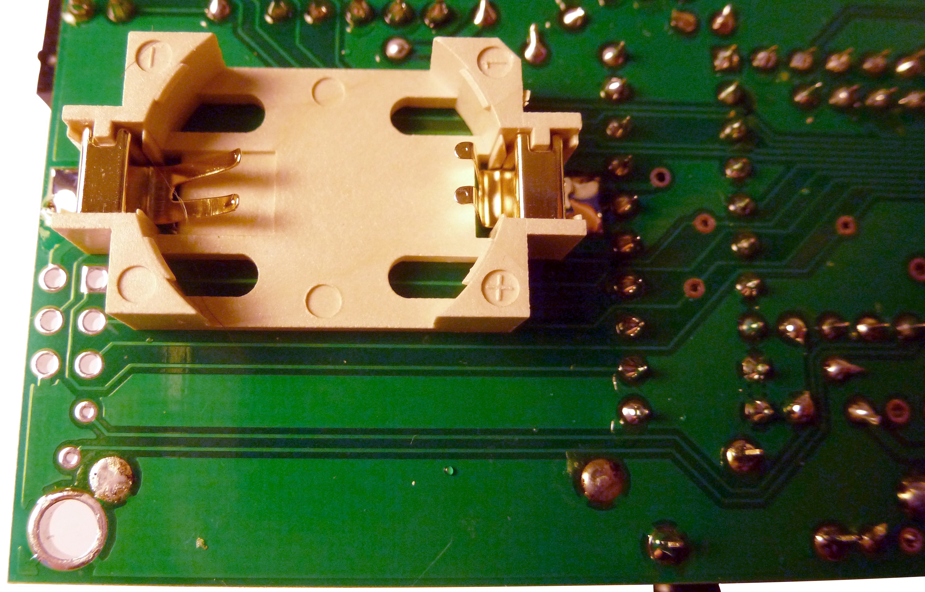
|
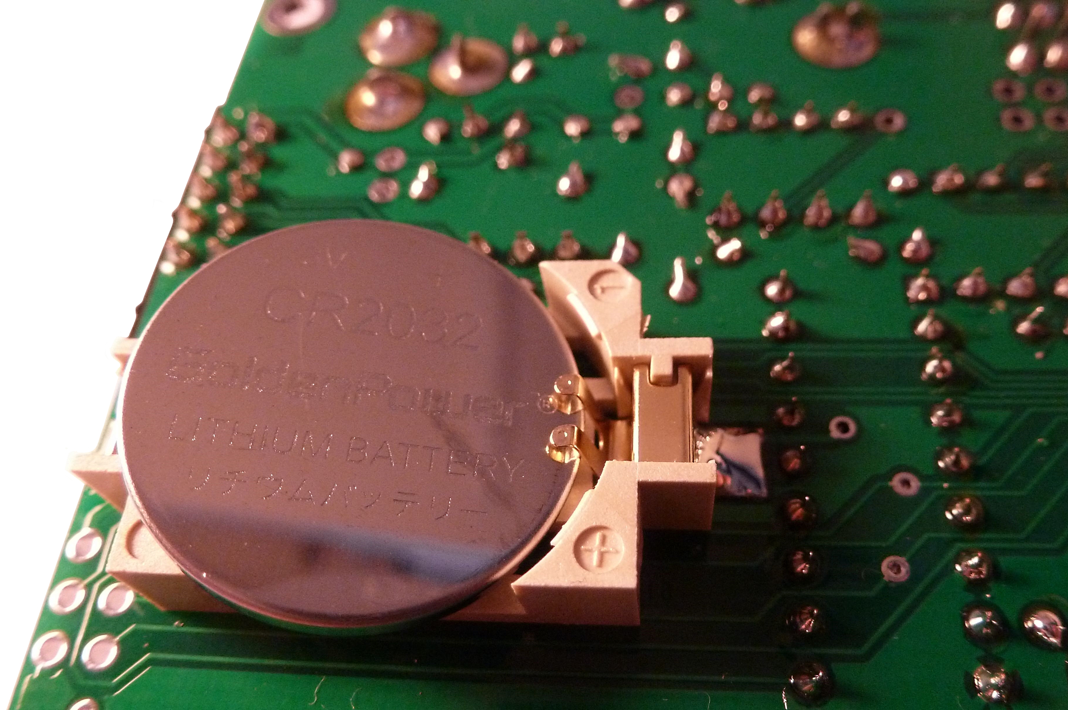
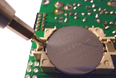
CR2032 Battery holder, SMD |
Take care
to make sure that the positive and negative
terminals are placed correctly - the "+"
connection should be towards the centre of the PCB.
To reduce
the stress on the battery connections to the PCB,
you could apply a little glue to the battery holder
prior to soldering. |
 |
| 30 |
|
|
|
|
BT1 |
CR2032 Coin Cell battery |
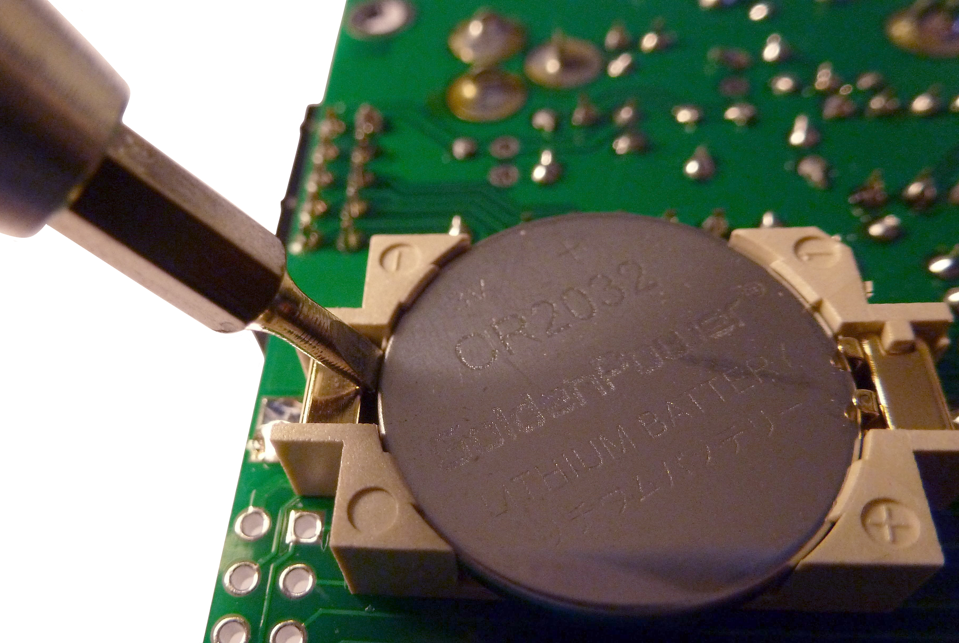
To plug
in the battery, place it so that it lays under the
two golden fingers at the right side, then press and
move the battery to the right until it snaps in. |
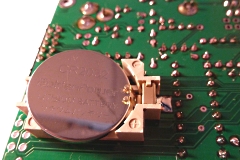 |
| Info |
|
|
|
To remove the battery, use a
flat screw driver to lever the battery out of the
holder.
The screw driver / lever should move the battery
to the right and upwards at the same time. |
 |
| 31 |
|
|
|
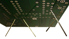
| |
M3 spacer bolts, internal thread, 18 mm |
|
|
M3 distance sleeves, 8 mm |
These parts are intended for mounting the
display, however, even if not using the display,
the legs will provide a stable base of the unit.
|
 |
| 32 |
The
cathode (shorter lead, flattened side of the LED)
goes into the square box on the PCB, both on the
left side. |
 |
| 33 |
The next
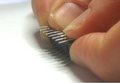
step is to fit the ICs into their sockets.
The legs
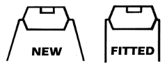
on new chips have their legs slightly splayed, they
need to be bent slightly so that they fit into the
sockets (or directly into a PCB)
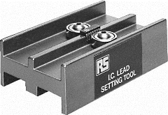
Images from RS-Components |
 |
| 33 |
I have one of these - it's an IC lead setting
tool, the tool can dress the legs of 0.3" and 0.6"
ICs. The tool does a really good job, but it's only
shown here so that I can flaunt mine :-) |
 |
| 33 |
The same effect can be achieved by carefully
bending the legs on one side at a time on a flat
surface.
(Photo from
instructables.com) |
 |
| 33 |
| Install the ICs in their
sockets |
| IC1 |
ATmega1284P-PU |
| IC2 |
SN75160BN |
| IC3 |
SN75161BN |
| IC4 |
74LVC245A |
|
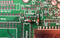
IC5 |
PCF8583 |
(Required for RTC only) |
|
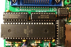 |
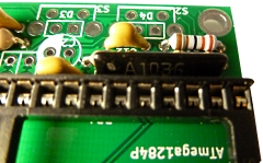
| 33 |
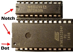
Take care to align the "notch" in the end of the
IC with corresponding notch printed on the PCB at
each IC. Check that every pin on each IC has been
properly inserted into its socket. |
 |
| LCD
Assembly / Fitting |
|
Seq. No. |
Description / notes |
Photo |
|
|
| Pin Number, Left to
right, facing front (unmarked) |
| 1 |
Vss |
(0V) |
| 2 |
Vdd |
(+5V) |
| 3 |
Vo |
(For LCD) |
| 4 |
RS |
(Register Select) |
| 5 |
R/W |
(Not Used) |
| 6 |
E |
(Enable) |
| 7 |
DB0 |
(Data 0 - not used) |
| 8 |
DB1 |
(Data 1 - not used) |
| 9 |
DB2 |
(Data 2 - not used) |
| 10 |
DB3 |
(Data 3 - not used) |
| 11 |
DB4 |
(Data 4) |
| 12 |
DB5 |
(Data 5) |
| 13 |
DB6 |
(Data 6) |
| 14 |
DB7 |
(Data 7) |
| 15 |
A |
(LED Anode) |
| 16 |
K |
(LED Cathode) |
|
 |
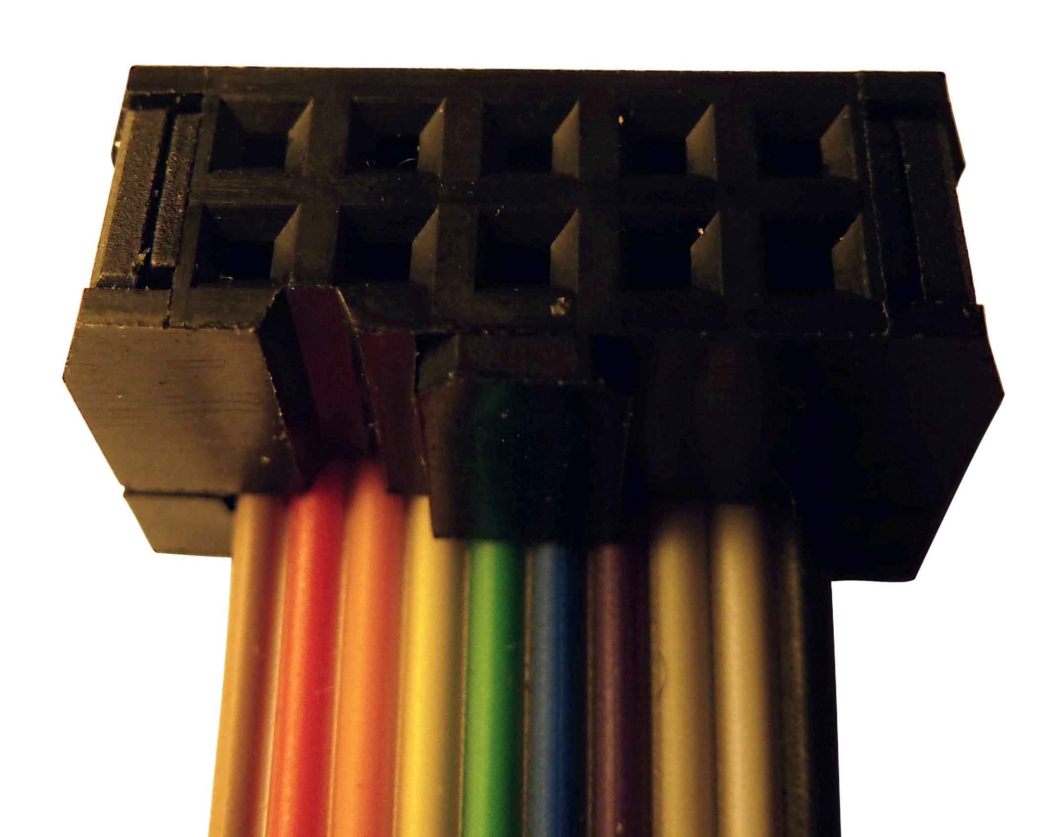
| a |
|
|
|
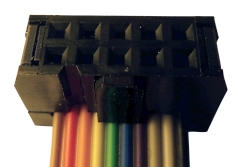
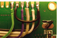
Interconnection between the PCB and the display uses
a 10-way ribbon cable, fitted with an IDC connector
at the PCB end, and soldered directly to the back of
the display at the other.
When it
has been fitted, the cable is not subjected to any
significant strain, so a low profile connector,
i.e., one with no strain relief clip fitted, is
preferred, since there is limited clearance between
the PCB and the display.
Note the
orientation of the cable with respect to the key on
the plug |
 |
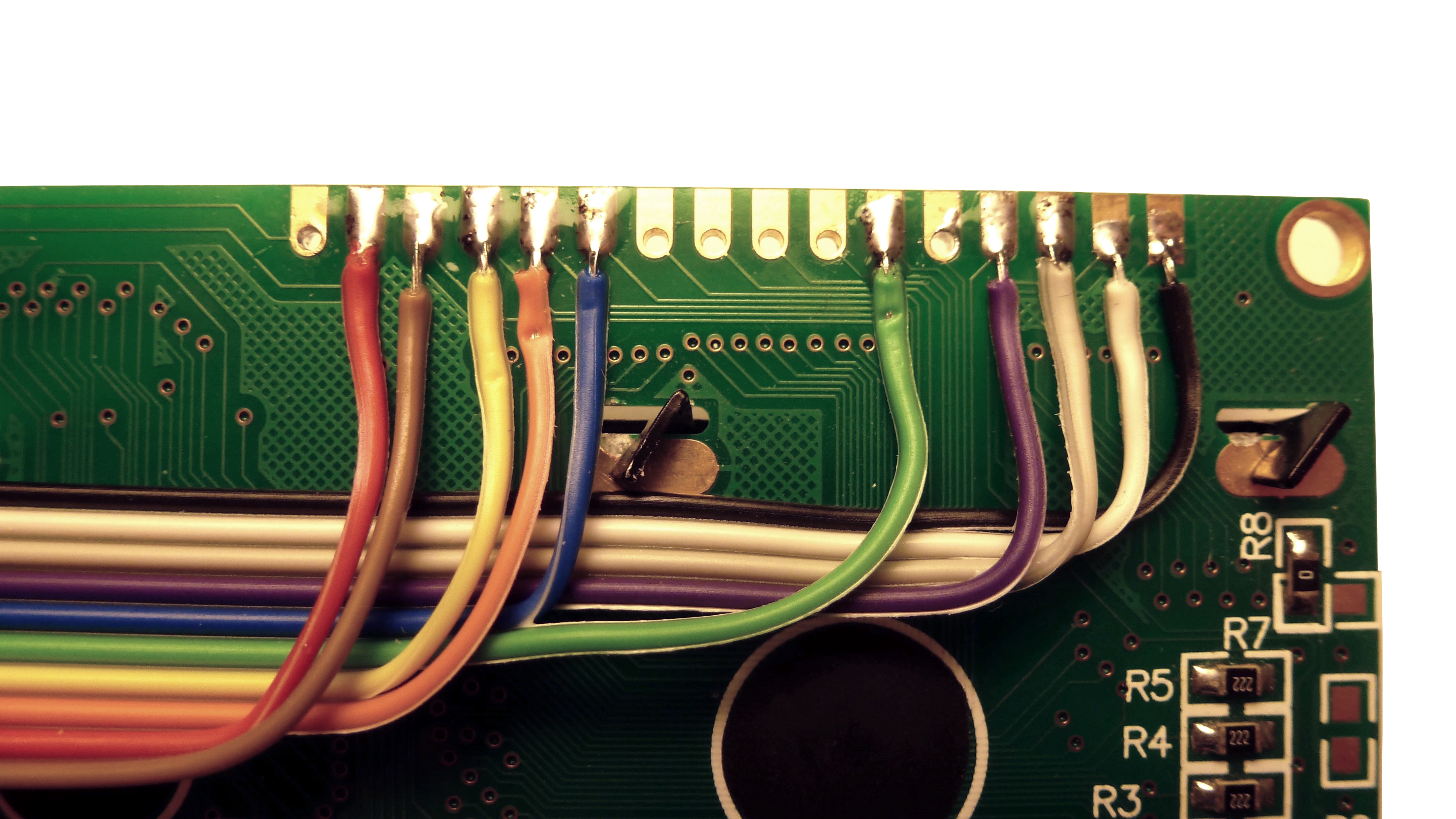
| b |
|
|
|
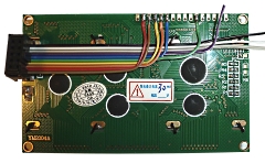
Lay the ribbon cable on the underside of the
display with the IDC plug connector facing towards
you and the dimple facing the centre of the display
PCB. Obviously, you need to make sure that the
cable is long enough to mate with the petSD+ PCB
header, but leaving it too long will make it
difficult to fit the display on top of the PCB. |
 |
| c |
|
|
|
Close up of the connections |
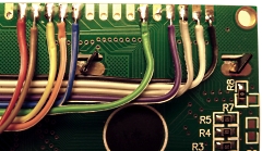 |
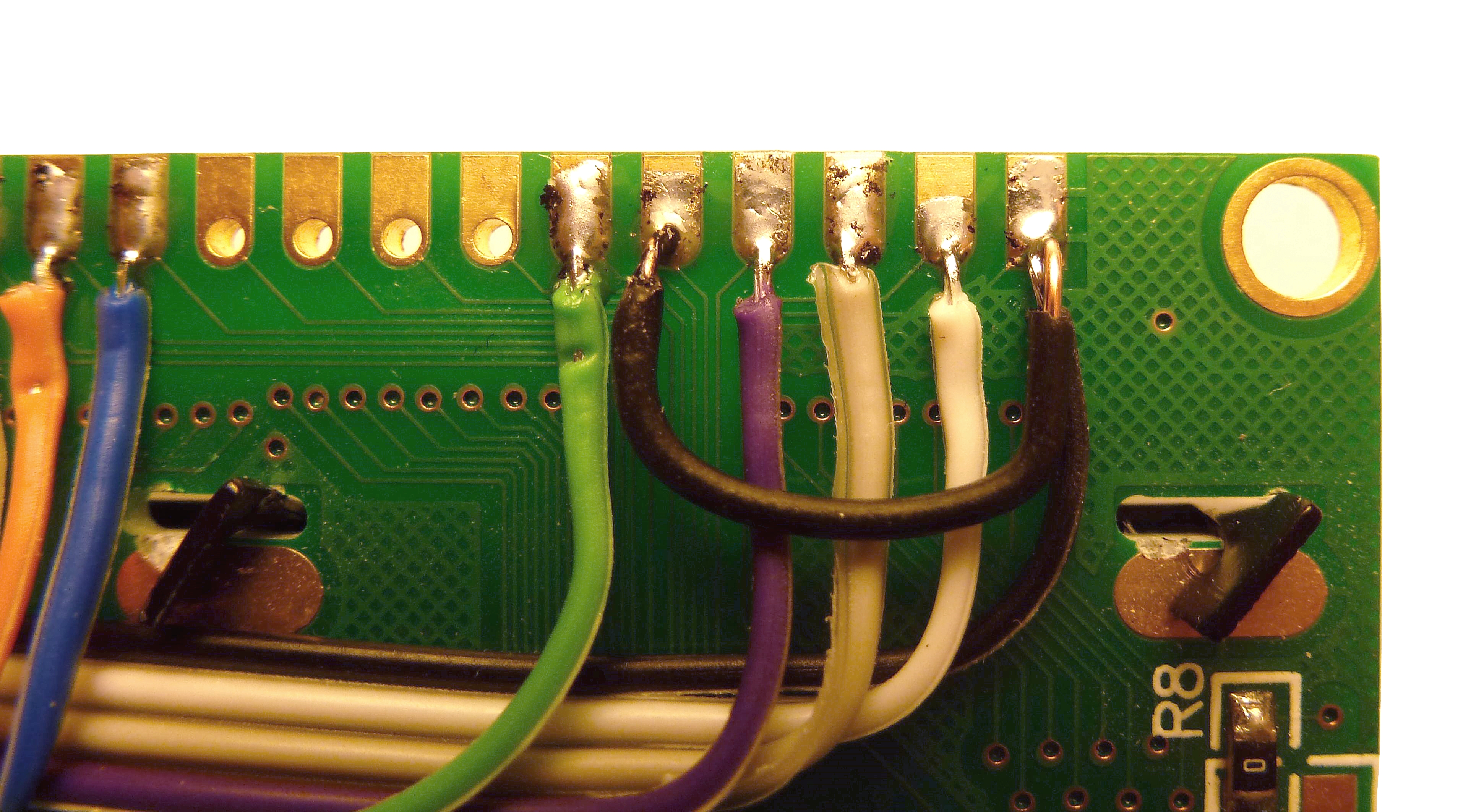
| d |
|
|
|
Add a shorting link between the terminals shown |
 |
| e |
|
|
|
As described in step 8, R2 is
best placed on the LCD itself, rather than on the
petSD+ PCB. Solder the resistor across terminals 1
and 16 on the front of the LCD as shown. (See the hardware page
for how to determine the correct value of R2, it
should normally be in the 3R to 6R range.) |
 |
| f |
|
|
|
Plug the display cable into the mating connector
on the petSD+ PCB (P5) and fix the display to the M3
spacer bolts using the M3 pan head screws. |
 |
|
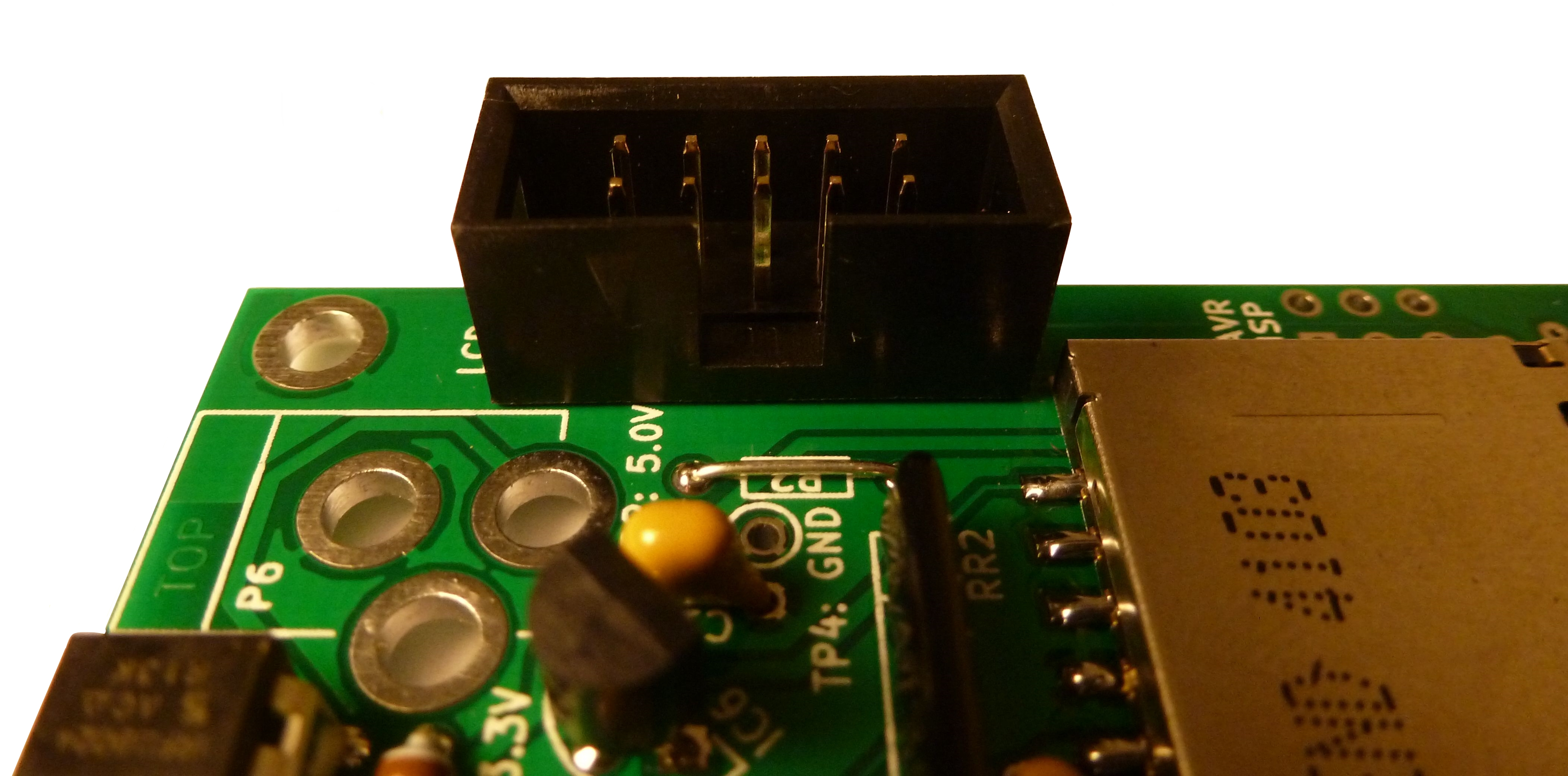
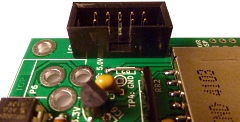
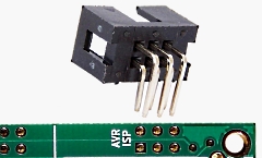
ISP
Port Connector |
|
Seq. No. |
Description / notes |
Photo |
| ISP |
Should you wish to fit the ISP port connector, a
convenient point in the assembly would be at the
same time as P5 is installed (step 22.
Alternatively, the connector can be added after the
board has been completed. Note, to allow a
programmer to be connected, the connector will
protrude beyond the edge of the board and should be
mounted orientated as shown. |
 |
| Debug
Message Logging (Development Tool) |
|
|
Description / notes |
Photo |
| |
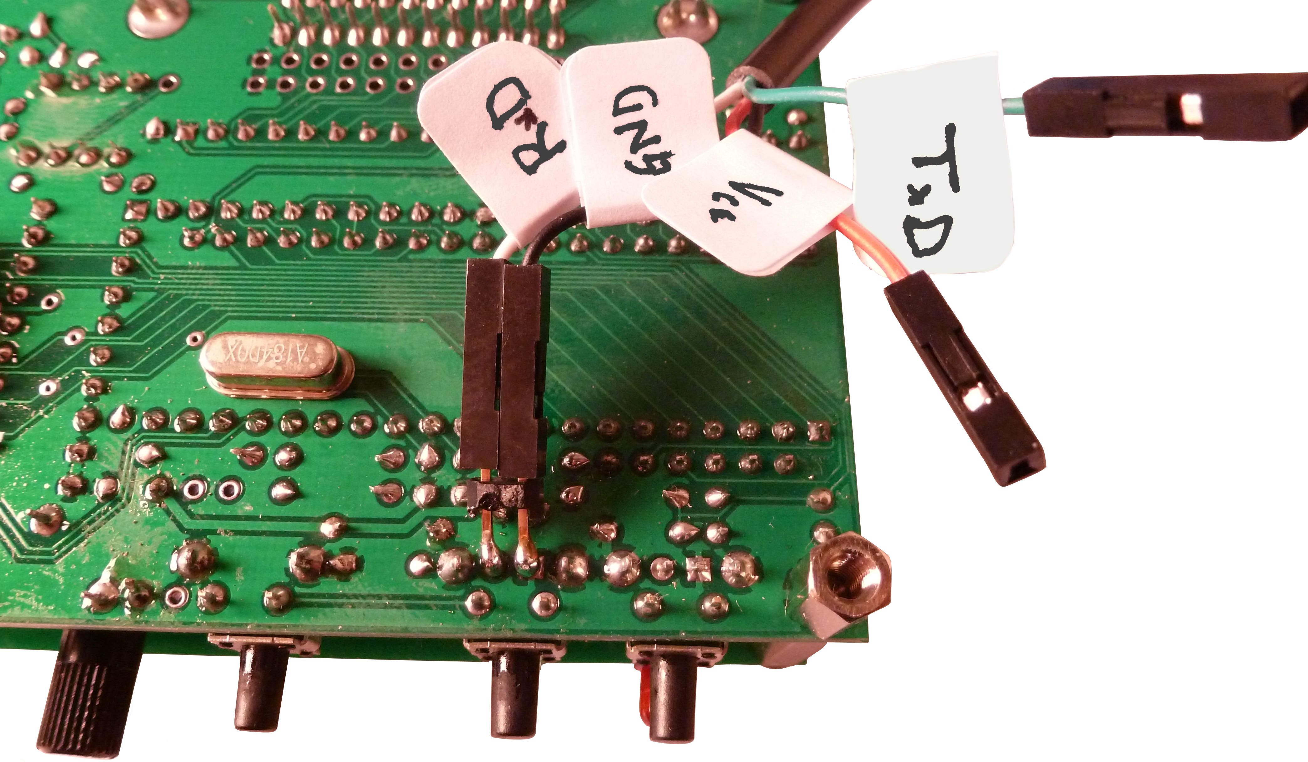
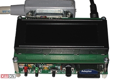
It is possible to configure petSD+ to write
debug messages that can be logged to a TTL level RS232
type serial
port.
The serial line shares the port with the green
LED and debug output is enabled by setting
CONFIG_UART_DEBUG=y in configs/config-petSD+ (a
compile-time option). |
 |
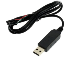
| |
Modern PCs are rarely fitted with a TTL RS232 port,
but USB converters are readily available.
One example, and the one used by Nils , is shown
here, it uses a PL-2303HX USB to Serial Bridge
Controller. It is available from ebay sellers for as
little as £1-£2 |
 |
|
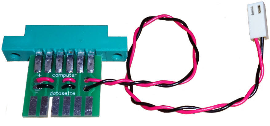
Internal Mounting Suggestions |
|
|
Description / notes |
Photo |
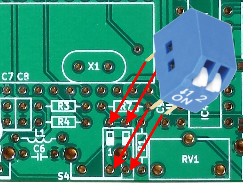
| Style |
|
DIP-SW2 |
2-way DIP switch (optional) |
If petSD+ is to be mounted internally, the LCD
and image selection switches would not be required
and a 2-way piano dip switch can (optionally) be
installed to configure the IEEE-488 device address
from 8-11 in the same way as was done with a
Commodore 1541-II drive |
 |
| Style |
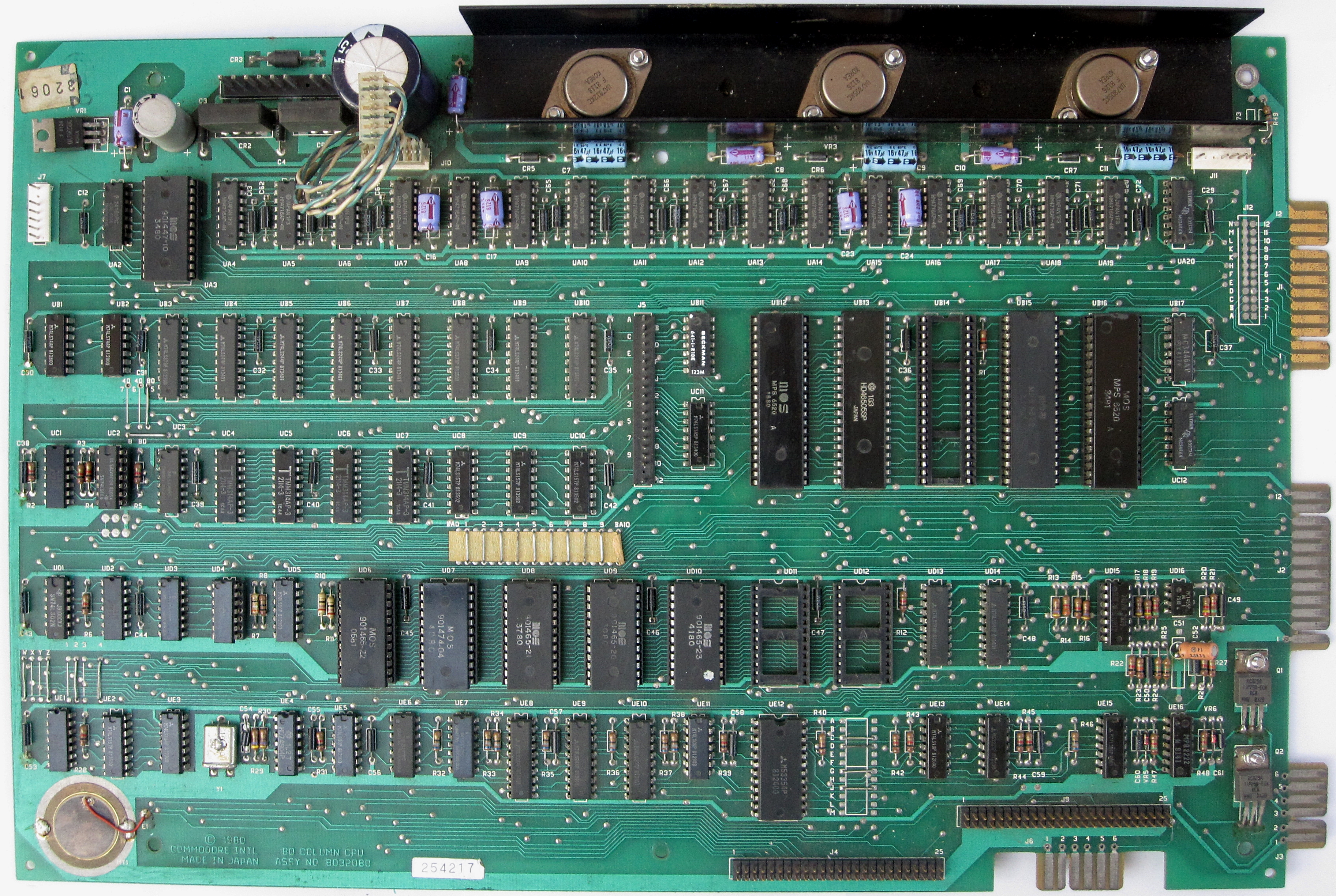
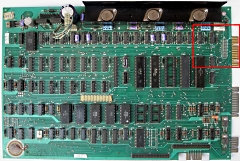
The system board used in CBM 8032/8096 (not SK)
computers has an internal pin header ("J12")for
the IEEE-488 port, adjacent to "J1", the edge
connector for the external IEEE-488 port.
On the PCB in my machine shown here, the header
position is not populated, so a 2x12, 0.1" pitch,
pin-header would need to be installed to allow the
internal petSD+ to be connected internally. |
 |
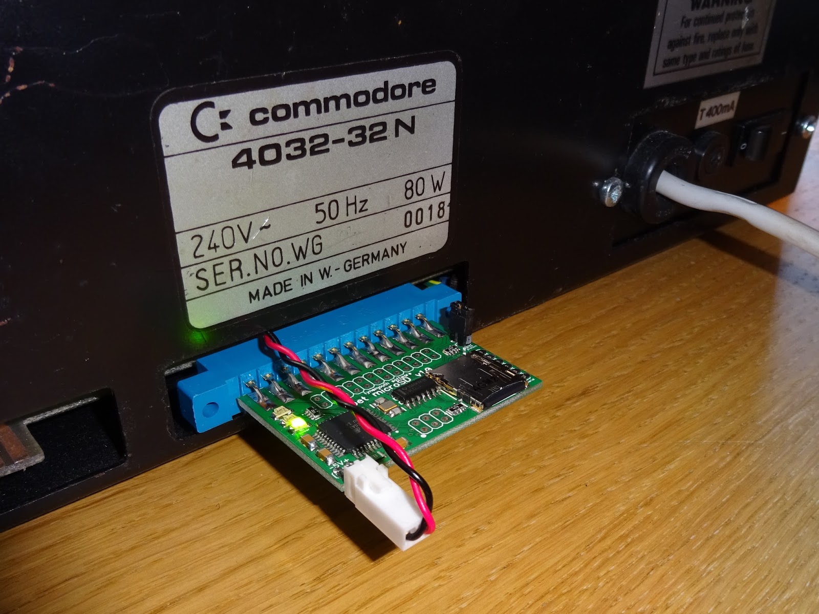
| Style |
If the white connector ("J11") is fitted to the
system board, but not used, it could supply power to
petSD+, on my machine though, it is used to provide
power to the 64kB RAM board that sits above the
system board. |
 |
| Style |
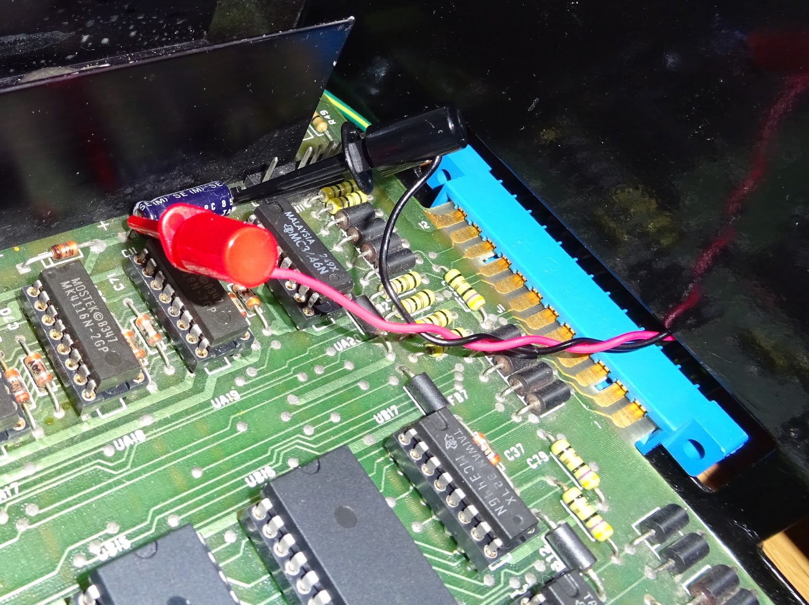
When mounting petSD+ internally, another option would be to copy the solution
that Dave Curran uses for some of his
petMicoSD offerings and use a couple of test
clips to pick up power from a convenient point on
the PET PCB, such as "C11", or somewhere
closer to where your petSD+ will be located.. |
|
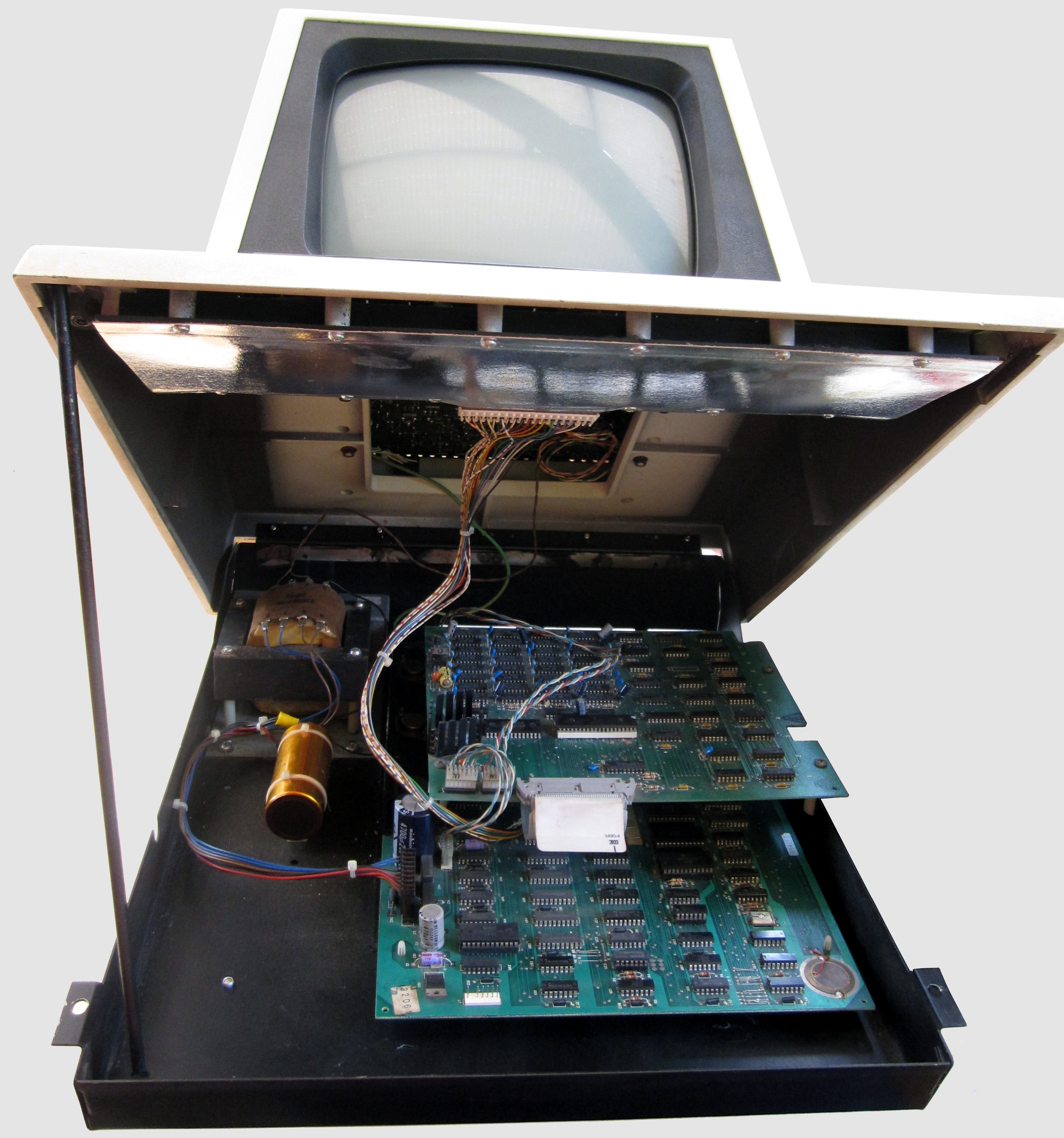
| Style |
As shown in this photo, there is lots of free
space inside a CBM 8032/8096 to locate a petSD+.
As is it highly unlikely that you will be moving
your machine around a lot, it may be acceptable to
just place the petSD+ board in the empty space at
the front left of the case - suitably
insulated from the metal base of the
computer.
|
 |
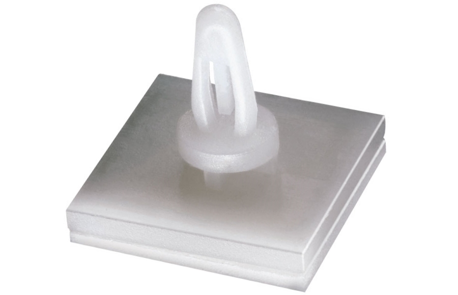
| Style |
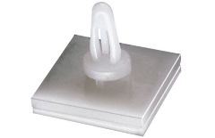
Alternatively, a better option would be to use
self adhesive PCB supports like this to fix the
petSD+ PCB to the base off the computer, raising it
off the bottom to provide clearance for the battery
holder (if fitted) and protecting against the solder
side of the board from making contact with the case. |
 |
|