|
 |
Commodore PET Projects
- petSD+ |
petSD+ - Hardware
 |
 |
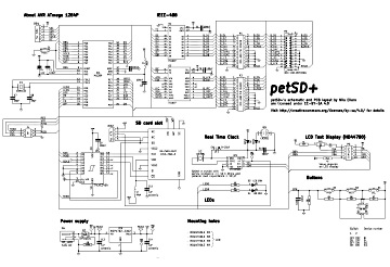
| petSD+ Draft Schematic |
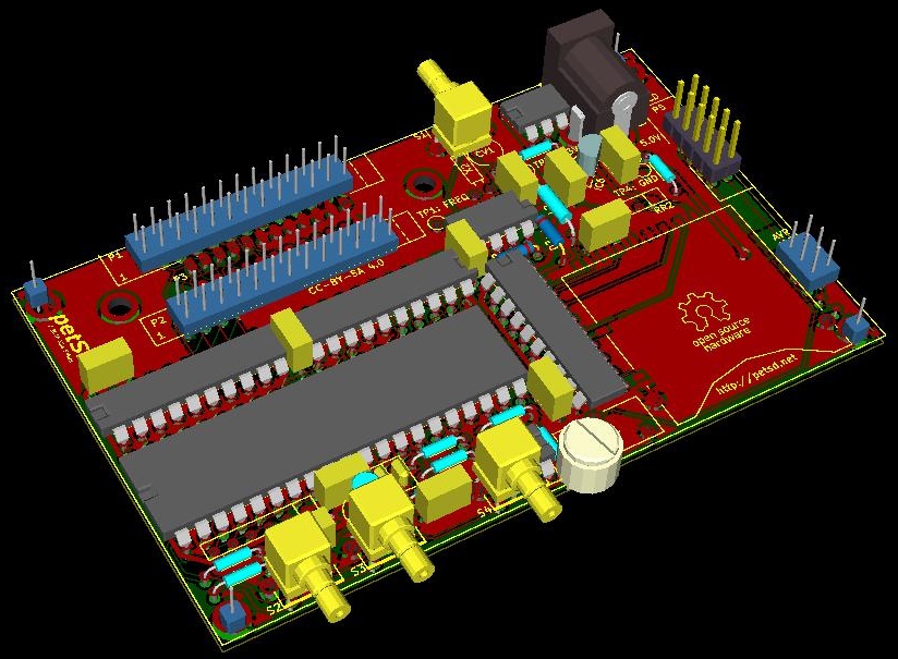
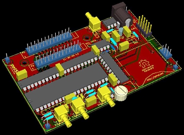
PCB 3D model |
The hardware is built around an
Atmel
ATmega
1284P
AVR microcontroller (MCU)
with 128KB of
flash
memory, 16 KB of
SRAM and a 4 KB
EEPROM,
clocked at 18.432 MHz. To make assembly easier for electronic
hobbyists, the
PDIP package was chosen for the petSD+ design . The main
components on the petSD+ PCB are :
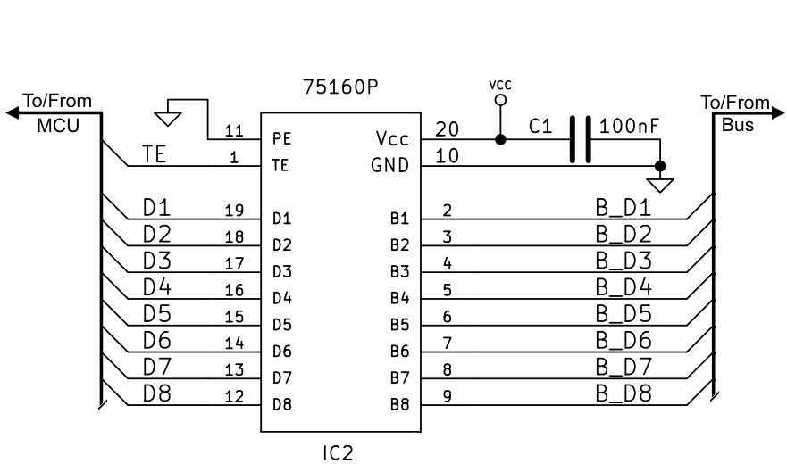
Bus Drivers
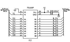
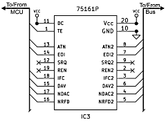
To enable petSD+ to coexist with other devices on the
IEEE-4888 bus, it is fitted with a pair of Texas Instruments
SN75160/SN75161 IEEE-488 bus drivers, controlled by the MCU.
| The SN75160 8-channel IEEE-488 (GPIB)
transceiver is designed to support two-way
communications for the 8 data bits of the parallel
IEEE-488 bus using two control pins, TE (Talk
Enable) and PE (Pull-up Enable). In petSD+, TE is
controlled by the MCU and PE is tied to 0V. |
 |
| With PE tied low, the driver outputs behave as
passive pull-ups when TE is high and are placed in
the high impedance state when TE is low. |
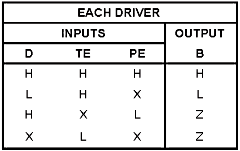 |
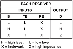
| When TE is low, the receiver bits are set to the
values of the corresponding bus data bits. |
 |
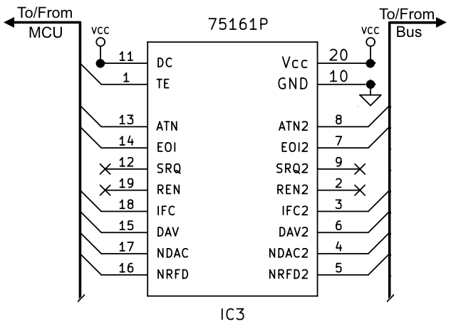
| The SN75161 8-channel IEEE-488 (GPIB)
transceiver is designed to provide the bus
management and data-transfer signals for a single
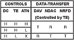
controller IEEE-488 bus system.
The direction of data is controlled by the
Direction Control (DC) and Talk Enable (TE) pins. In petSD+, TE is controlled by the MCU and DC is
pulled up to Vcc. This means that petSD+ will always
be a device and never a bus master
such as a CBM computer. In other words: you can use
it only as a device attached to a computer but never
"stand-alone" with other IEEE-488 devices. |
 |
|
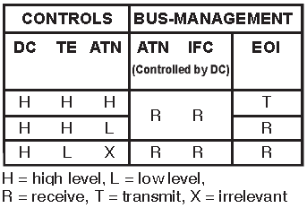
In petSD+, the Service Request (SRQ) and Remote
Enable (REN) bus management channels are not used.
With DC pulled high, the remaining bus management
channels, Attention (ATTN), Interface Clear (IFC)
and End or Identity (EOI) are set to the directions
shown in the reduced function table opposite :
(Transmit means that petSD+ writes to the IEEE-488
bus)
(Receive means that the IEEE-488 bus state is
written to petSD+ ) |
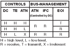 |
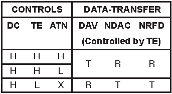
| With DC pulled high, the data transfer
channels (used for
handshaking), Data Valid (DAV), Not Data
Accepted (NDAC) and Not Ready For Data (NRFD) are
set to the directions shown in the reduced function
table opposite : |
 |
Level Shifter
Since the petSD+ design uses both +3.3VDC (for the SD Card)
and
TTL voltage levels (for the other ICs), there needs to be
voltage level shifting to convert signal between +5V and
+3.3V for the SD card interface. The
74LVC245A
Octal Bus Transceiver (IC4) is used to provide level conversion
for the SD Card interface signals highlighted in the
table below :
|
74LVC245A |
74LVC245A |
SD
Card (SPI Bus Mode) |
|
| Pin |
Name |
Connection |
Pin |
Name |
Connection |
Pin |
Name |
Function |
| 2 |
A0 |
SCK |
18 |
B0 |
CLK |
5 |
CLK |
Serial Clock |
| 3 |
A1 |
MOSI |
17 |
B1 |
DI |
2 |
DI |
SPI Data In |
|
4 |
A2 |
Ground |
16 |
B2 |
n.c. |
- |
- |
- |
| 5 |
A3 |
SDCS |
15 |
B3 |
CS |
1 |
CS |
SPI Card Sel |
|
6 |
A4 |
Ground |
14 |
B4 |
n.c. |
- |
- |
- |
|
7 |
A5 |
Ground |
13 |
B5 |
n.c. |
- |
- |
- |
| 8 |
A6 |
D0 |
12 |
B6 |
MISO |
7 |
DO |
SPI Data Out |
|
9 |
A7 |
Ground |
11 |
B7 |
n.c. |
- |
- |
- |
Real Time Clock
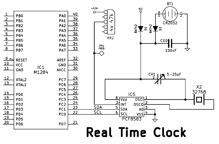
The Real Time Clock is implemented using an
NXP
PFC8583 clock and calendar chip, interfaced to the MCU using
the
I2C
bus. A 32.768 kHz quartz crystal is connected to the
RTC OSCI and OSCO pins. A trimmer capacitor between OSCI and VCC
is used for tuning the oscillator.
The PFC8583 data sheet states that "average deviations of ±5
minutes per year are possible", this equates to around 1.5
seconds per day, or expressed another way, around 19
parts-per-million (ppm). The oscillator supplied specified for
use in petSD+ has a tolerance of 20 ppm on its own, but is only
one contributor to the overall tolerance, other variables
include the capacitor tolerance and temperature.
There are a few ways of using the trimmer capacitor to adjust
the clock rate if the variance of your device is greater than
this, the easiest are :-
Both of these are constrained by the
accuracy of the test equipment being used.
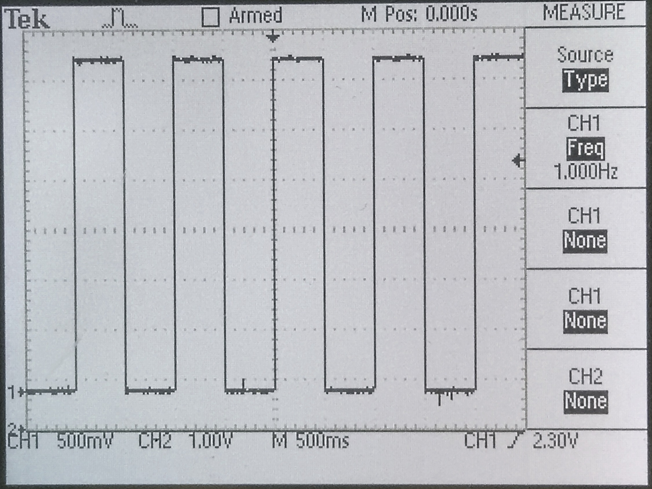
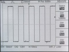
For models with the Real Time Clock option, test
point TP1 on the PCB can
be used to measure the clock "tick" rate.
This photo is of the display on my 'scope when
measuring the frequency at TP1 for the first petSD+
that I built. As you can see, it is a nice, clean,
square wave, with a frequency of 1.000 Hz, i.e., 1
cycle/second as it should be. |
 |
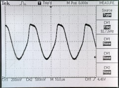
This photo is of the raw signal from the 32.768
kHz oscillator connected to the Real Time Clock chip
oscillator input on pins 1 & 2, the measured
frequency at this point was 32.72 Khz.
This
is quite a bit outside the stated tolerance of the
oscillator (20ppm) but takes no account of other
variables and is limited by the accuracy of the
'scope. |
 |
Power Supply
and Voltage Regulator
The raw +5VDC power supply to the petSD+ PCB is fed to an
IRFD9024
power
MOSFET, used to provide reverse polarity protection for the
PCB.
In addition to the +5VDC supply, petSD+ requires +3.3VDC for
the SD
Card as specified by the SD Card standard. A
MCP1702-3302 voltage
regulator is used to generate the +3.3VDC supply used by the SD
Card slot and the
74LVC245A
voltage level shifter.
SD Card Slot
The card slot used in petSD+ is an
Attend 104H-TDA0-R, it is a surface mount component, but
with care, can be hand soldered onto the PCB, after
installation, it should have been tested as described in the
Assembly instructions.
During testing and normal operation, you will probably find
that SD card insertion and removal feels a little "rougher" than
with other SD card slots that you use, whilst this is unusual,
it appears to be the norm for this particular card slot. The
issue is present on the petSD+ prototypes that Nils has built
and the boards that I have assembled.
Nils has made this observation : "There's a little black
plastic finger on the left side that gives this first resistance
when inserting the card. Just out of curiosity, I broke that
finger away at one slot and looked what happened: it turned out,
this finger is used to hold the card and prevent them from just
pulling it out once it is inserted. I never experienced this on
any other SD slot I have anywhere, it really feels kind of
broken, but that's just the way this "special" slot is."
In the absence of a more technical description, I have found
that giving the card a little "wiggle" during insertion and
removal seems to make the process slightly easier.
SD Card Slot Pin-Out
| |
SD
Card (SPI Bus Mode) |
|
| Connection |
Pin |
Name |
Function |
| SDCS |
1 |
CS |
SPI Card Sel |
| MOSI |
2 |
DI |
SPI Data In |
| |
3 |
VSS1 |
Ground |
| |
4 |
VDD |
+3.3 VDC |
| SCK |
5 |
CLK |
Serial Clock |
| |
6 |
VSS2 |
Ground |
| MISO |
7 |
DO |
SPI Data Out |
| |
8 |
n.c. |
- |
| |
9 |
n.c. |
- |
| IC1 Pin 19 |
CD |
CD |
Card Detect |
| IC1 Pin 20 |
WP |
WP |
Write Protect |
| |
SC |
SC |
Signal Common |
LCD Module
petSD+ was designed to allow an (optional) 20 character x 4
line LCD display to be mounted above the PCB. The LCD driver
code in the NODISKEMU firmware is
programmed to drive displays fitted with an
Hitachi HD44780, or compatible, LCD controller in 4-bit
mode.
| HD44780 LCD Module
(or Compatible) |
|
Pin |
Symbol |
Connected To |
P5
Pin |
Function |
| 1 |
Vss |
Power Supply |
1 |
Signal Ground for LCM (Ground) |
| 2 |
Vdd |
Power Supply |
2 |
Power Supply for LCM (+5VDC) |
| 3 |
Vo |
Power Supply |
3 |
Contrast Adjustment |
| 4 |
RS |
MCU |
4 |
Register select signal |
| 5 |
R/W |
MCU |
(1) |
Read/Write select signal (Forced Low) |
| 6 |
E |
MCU |
6 |
Operation (data read/write) enable signal |
| 7 |
DB0 |
n.c. |
n.c. |
Not used in 4 bit operation |
| 8 |
DB1 |
n.c. |
n.c. |
Not used in 4 bit operation |
| 9 |
DB3 |
n.c. |
n.c. |
Not used in 4 bit operation |
| 10 |
DB3 |
n.c. |
n.c. |
Not used in 4 bit operation |
|
11 |
DB4 |
MCU |
5 |
Data transfer from MCU to LCM |
| 12 |
DB5 |
MCU |
8 |
Data transfer from MCU to LCM |
| 13 |
DB6 |
MCU |
7 |
Data transfer from MCU to LCM |
| 14 |
DB7 |
MCU |
10 |
Data transfer from MCU to LCM |
| 15 |
A |
Power Supply |
9 |
Backlight Power |
| 16 |
K |
Power Supply |
n.c. |
To Ground via current limiting resistor, R2 |
A wide variety of compatible displays are available, with
some slight variations between them; apart from obvious
differences such as colour, the displays have a pretty much
standard design. The most important difference relevant to petSD+
is the voltage used for the LCD backlight. In some displays, a
+5V backlight supply is fine, in others, +5V will damage the
display. Resistor R2 in the petSD+ design is provided to drop
the +5V supply used for the backlight down to the appropriate
voltage for a particular display. To allow the LCD to be
replaced with a different model, the preferred location for
mounting R2 is on the LCD itself.
In order to select the appropriate resistance and power
rating values for R2, we need to know the backlight supply
voltage and operating current for the LCD module being used. If,
for example, the supply voltage is 5V, the LCD backlight voltage is specified as 4.2V and
the operating current is 260mA
| Given the relationships : |
|
and |
|
| |
|
|
|
| |
|
|
|
| |
|
|
|
| |
|
|
|
|
|
|
Making a 3R, 1/4 W resistor suitable
for this display |
The contrast for the display is controlled by pot VR1, but
the fixed value of R2 sets the LCD to a fixed brightness level.
To some extent, the "ideal" brightness, and hence the choice of
resistor R2, is subjective. The fixed value supplied in my kits
or fitted to pre-assembled units, should give an acceptable
level of brightness for the majority of users, however, being
located on the top of the LCD, the resistor can easily be
replaced with a different value by the end user - subject to the
electrical specification of the display being respected.
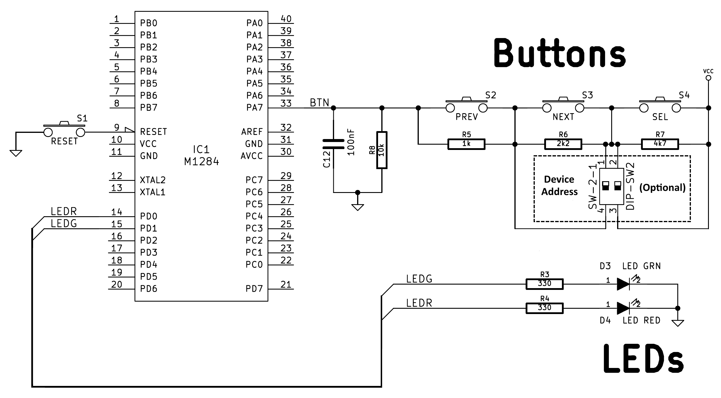
User Controls
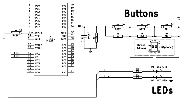
This simplified extract from the petSD+ schematic shows how
the User Controls are connected to the MCU.
All versions of petSD+ have a RESET push-button (S1) located
at the rear of the unit, close to the power connector. (Although
not shown here, the RESET button is also connected to the ISP
connector header pins.)
Internal models also have two bit-switches (SW2-1 & SW2-2)
installed, located at the front of the unit, close to the SD
Card slot. These are used to set the Device Address, the default
position, with both switches OFF, sets Device Address 8.
External models are intended to be fitted with the LCD screen
and three additional push-buttons, Previous (S2),
Next (S3) and
Select (S4), located at the front left hand side of the unit,
along with a potentiometer to adjust the display contrast.
Operation
of these controls is described on the
User Guide page.
The ATMega1284P has 4 x 8 channel I/O ports, giving a total
of 32 programmable I/O lines available to implement all of the
features in petSD+. A quick count of the I/O requirements for
petSD+ might suggest that the MCU did not have enough I/O
channels to do the job :
| Function |
Description |
Bits/Channels |
|
IEEE-488 data bus |
8-bit parallel port |
8 |
|
IEEE-488 control signals |
NRFD, NDAC, DAV, EOI, IFC, ATN,
TE |
7 |
|
LCD data bus |
4-bit data mode |
4 |
|
LCD control bits |
Enable, Register Select |
2 |
|
SPI
bus signals for CD slot and ISP port |
MISO, MOSI, SCK |
3 |
|
I2C
bus signals data for RTC |
Serial Clock (SCL) and Data
(SDA) |
2 |
| CD Slot status bits |
Card Detect, Write Protect |
2 |
| CD Slot control bit |
SD Card Select |
1 |
| LED outputs |
1 x Red, 1 x Green LED |
2 |
| Push-buttons |
Reset,
Prev[ious], Next,
Select, address select bits1 |
4 |
| Total I/O required |
|
36 ! |
However, Nils has used a neat trick to read the status of the
option buttons, this is made possible by the flexibility of the
MCU's I/O ports. As well as being configurable as bidirectional
digital I//O ports, each of the 4 ports also has an alternate
capability :
| MCU
Port |
Alternate Function |
| A |
8-Channel, 10-bit Analogue to Digital Converters, Pin change interrupts |
| B |
SPI Bus, AI comparator, Timer/Counter inputs, Pin
change interrupts |
| C |
JTAG signals, Timer/Oscillator, I2C
signals, Pin change interrupts |
| D |
Timer/Counter outputs, Pin change interrupts |
| (For details, see
the
ATMega1284P Datasheet) |
Nils has used one of the ADC channels on Port A to read the
status of the control switches as analogue values. A 10-bit ADC
has a count range from 0-1023, using the resistor network shown
in the schematic, the calculated voltages and corresponding ADC
values for all of the key combinations are shown in the table :
| Prev |
Next |
Select |
Voltage |
ADC |
Address1 |
| 0 |
0 |
0 |
2.79 |
570 |
8 |
| 0 |
0 |
1 |
3.79 |
775 |
9 |
| 0 |
1 |
0 |
3.18 |
650 |
10 |
| 0 |
1 |
1 |
4.55 |
931 |
11 |
| 1 |
0 |
0 |
2.96 |
605 |
n/a |
| 1 |
0 |
1 |
4.10 |
839 |
n/a |
| 1 |
1 |
0 |
3.40 |
695 |
n/a |
| 1 |
1 |
1 |
5.00 |
1023 |
n/a |
1
The schematic also shows the optional bit switches
used to set the device address for internal versions
of petSD+, these switches are wired in parallel with
the Next and
Select push-button pads on the PCB.
Later versions of the petSD+ firmware include diagnostics to
check the operation of the push-buttons as described on the
User Guide page.
Connectors
petSD+ does not connect directly to
a PET computer, the "standard" build of petSD+ is fitted with an
IEEE-488 connector like those found on PET disk drives. Most PET
and CBM computers use a cheap PCB edge connector to provide
IEEE-488 connectivity, to connect petSD+ or a Commodore disk
drive, you need to use a Commodore IEEE-488 disk drive cable
(hard to find) or a
PET to IEEE-488 adapter along with a standard IEEE-488
cable.
to be continued . . . . .
Board Revisions
|
Version |
PCB
Label |
Details |
|
1.1a |
1.1 |
Missing label for R10 added (no
change to PCB label) |
| 1.1 |
1.1 |
ISP MISO Issue fixed, resistor
R10 added (missing label) |
| 1.0 |
(none) |
First production board,
required fix for ISP MISO line |
| |
|
|
| |
|
|
|