|
"MTX Plus+" Video
Board

.
Software
The VDPs are controlled through a number of I/O
ports, for MTX and MSX computers (TMS9918), there are two ports,
a data port and a command port. The data port is used to read or
write single bytes to the Video RAM (the VRAM is not directly
accessible to the CPU, all read/writes must be through the VDP).
The command port is used to setup the data port address register
and to read/write one of the VDP registers.
MSX2 (V9938) and MSX2+ (V9958) use two
additional ports for access to the enhanced features of the VDP.
|
VDP Port |
Dir |
Function |
MTX |
MSX2 |
MTX+ |
Dir |
|
0 |
In/Out |
VRAM Data |
1 |
98h |
tbc |
Out/In |
|
1 |
In |
Set up data port address register |
2 |
99h |
tbc |
Out |
|
Write to VDP Register |
|
Out |
Read from VDP Register |
In |
|
2 |
Out |
Palette
Registers |
|
9Ah |
tbc |
In |
|
3 |
In |
Register Indirect Addressing |
|
9Bh |
tbc |
Out |
|
Out |
In |
To support software compatibility with the
MTX, the VDP must be capable of responding to Z80 I/O ports
1 and 2, for software compatibility with the original MSX,
the VDP must be capable of responding to Z80 I/O ports 98h
and 99h and for compatibility with MSX2/MSX2+, the VDP must
be capable of responding to Z80 I/O ports 98h to 9Bh.
I/O Port Address Decoding
The modularisation of MTXPlus+, coupled with
the desire to minimise the number of signals on the system
bus drove the decision to perform I/O address decoding on
the individual I/O cards, rather than centrally as in the
original MTX design. The draft design for the MTXPlus+ video
board was based on the use of discrete TTL logic to decode
the VDP and CSG I/O addresses.
However, since
Lez's kits of Z80 parts
included a number of GALs, address decoding will be done
using a GAL, greatly reducing the chip count on the video
board. This also makes it possible to easily reconfigure the
I/O port addresses for the MTXPlus+ video board so that they
do not clash with the original MTX port numbers, and
therefore, allows the video board to be tested on an MTX
computer before the MTXPlus+ CPU board is available.
Hardware
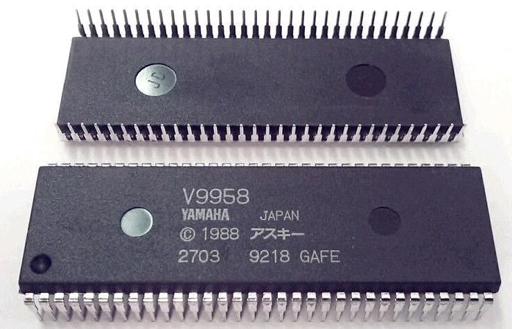
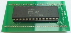
The V9958 was manufactured in a 64 pin
shrunken DIP (SDIP) package, the legs on this package have a hole
pitch of 0.07" rather than the 0.1" of a normal DIP
component. Whilst this would not be a problem for a custom
made PCB, it does mean that they are not directly compatible
with prototyping boards which presented a little bit of a
problem.
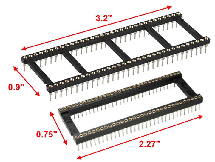
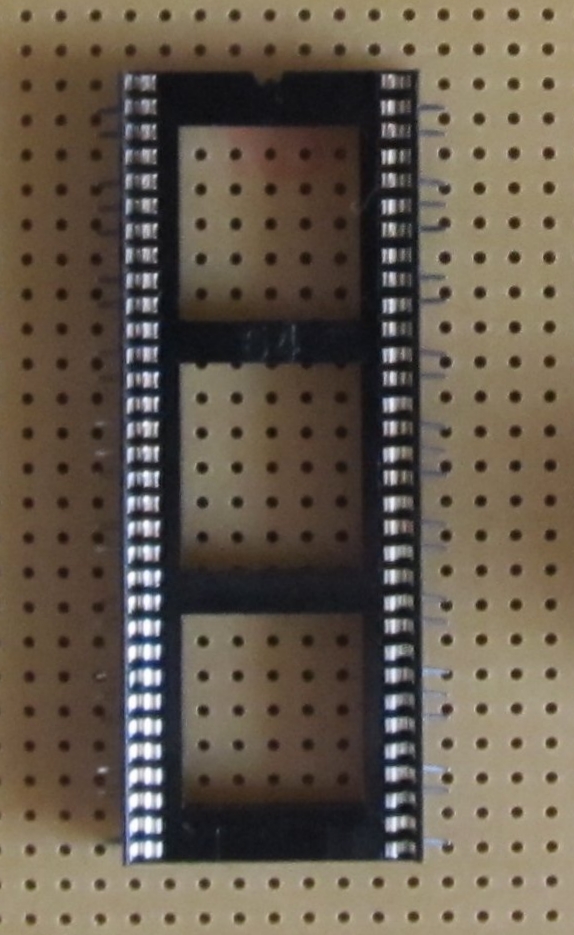
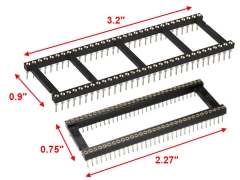
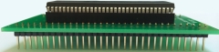
| The image shows the comparative sizes of sockets
for a 64 pin, 0.1" x 0.9" DIP package and an SDIP 64
socket. It can be seen that the footprint of
an SDIP package is much less than a standard DIP, in
this case, about 40% less.
This reduced space would have a cost benefit when producing
PCBs, but presents some difficulty when developing
prototypes such as the MTXPlus+ video board. |
 |
| It would be relatively easy, and not too
expensive, to get an adapter board manufactured to
allow an SDIP64 to be mounted on 0.1" pitch
prototype boards.
I am considering getting this made, it would not
only be useful for MTXPlus+, but would also help in
any other designs that we may do that uses one of
the V9958s that Lez has supplied.
In the meantime though . . . . . . |
 |
| Martin has worked out a way to "force-fit" an
SDIP-64 socket onto 0.1" prototyping board,
describing it, he says :
"Running from pin 1, 1 fits, pin 4 is at 0.21”
and is close enough to fit the 0.2” hole, the 8th
pin at 0.49” fits through the hole at 0.5”, and the
sequence begins again with the 11th pin. That gives
3 pins in 7 holes on the inner row, and 7 holes on
the next row out to feed wires through for the other
7 connections keeping it relatively neat." |
 |
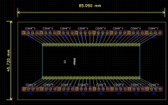
|
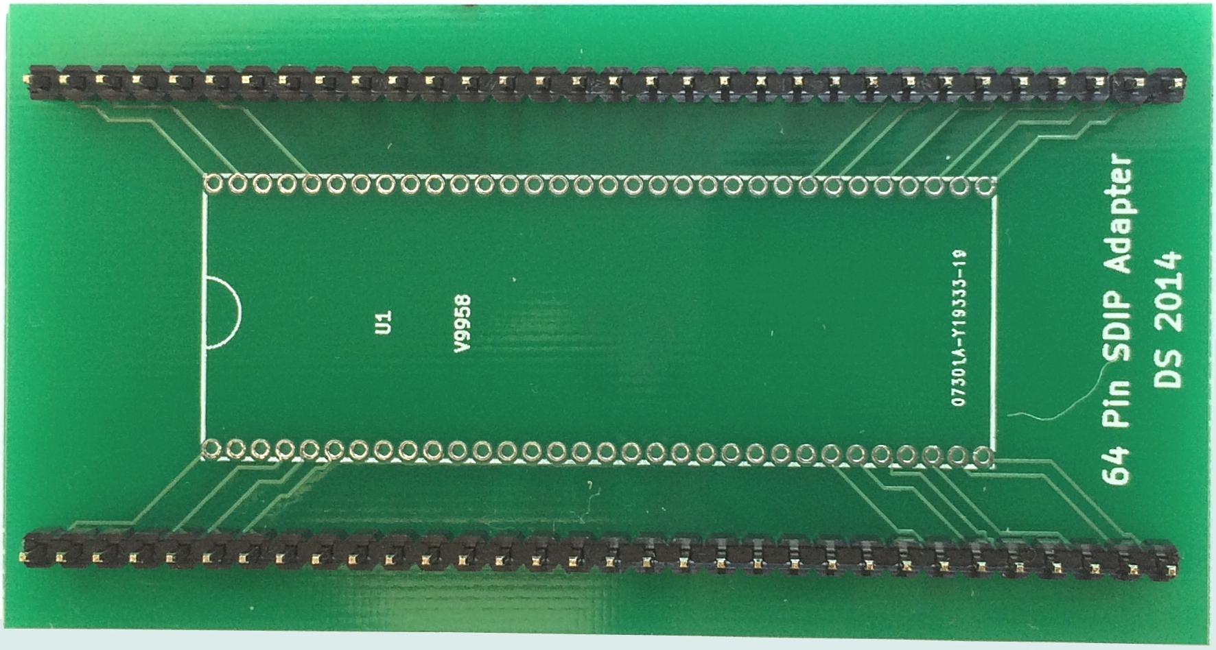
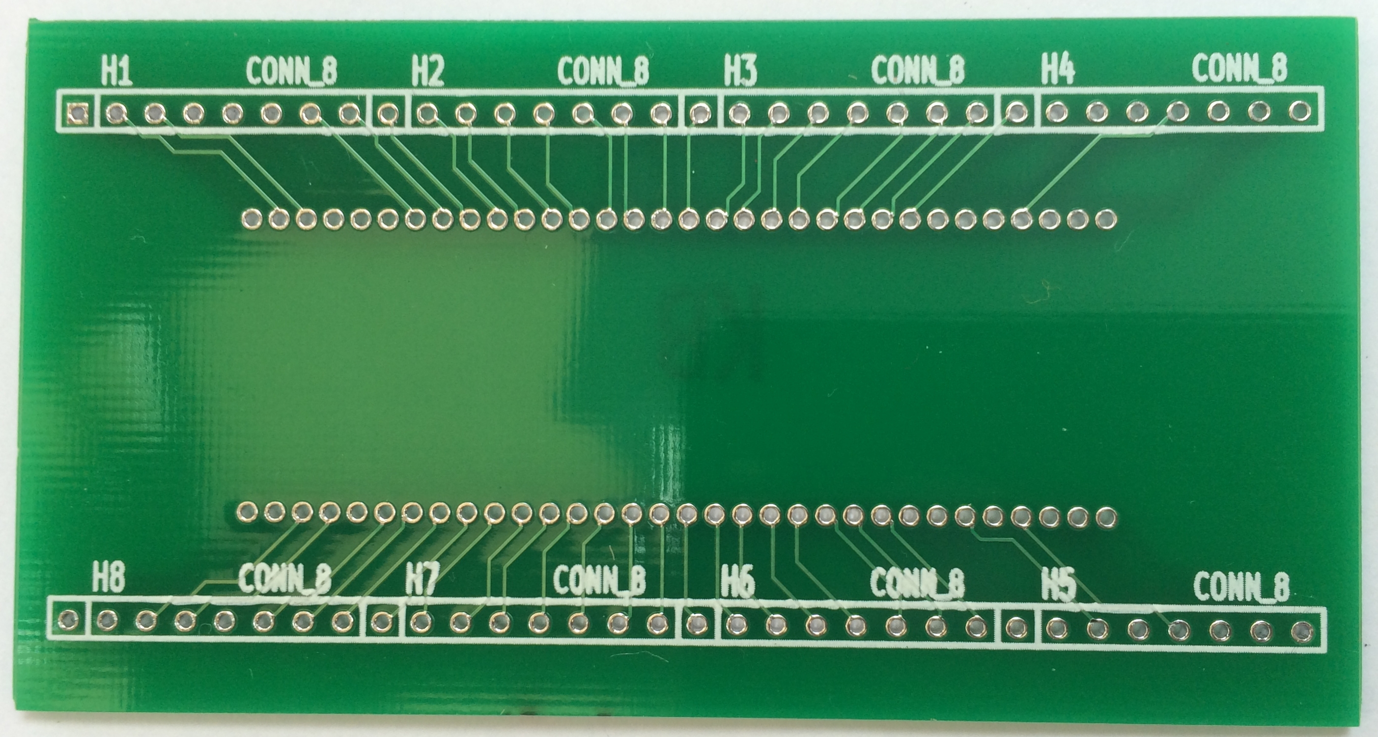
SDIP
64 Adapter Board
I decided to go ahead
and get some adapter boards made - here is the
result. |
| I was a bit concerned about putting the rows of
pins too close together, but having seen the board,
I could have reduced the distance between them, as
well as the distances to the edge of the board,
making it perhaps 10-15mm narrower - maybe next
time. [Update: Version 2 of the design ordered,
which is 0.5" narrower] |
 |
| I did a little tweaking of the pad sizes
for the SDIP pins to give a little more clearance
between them for hand soldering, as you can see,
they are still very close, but the spacing should be
OK. There is a minor cosmetic issue - I meant to
delete the header connector IDs from the board as it
looks messy, but I forgot. |
 |
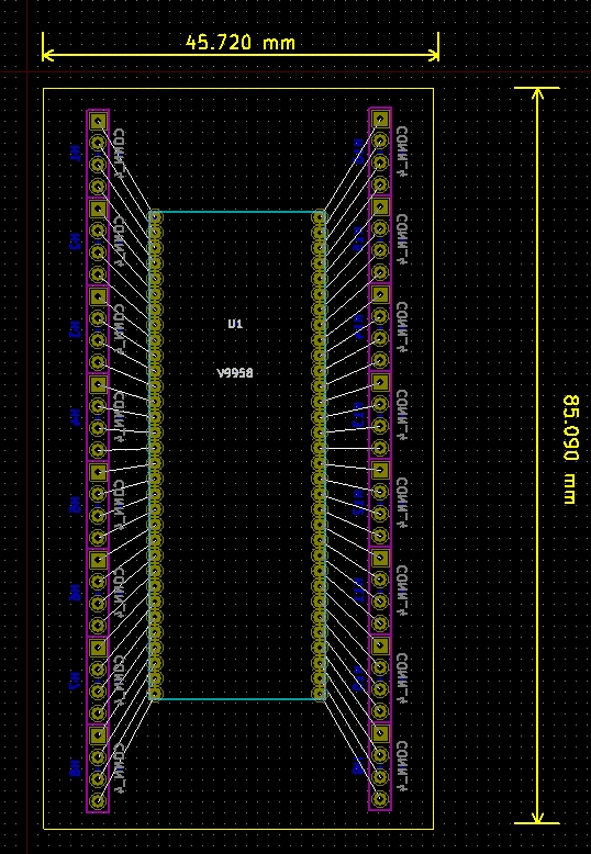
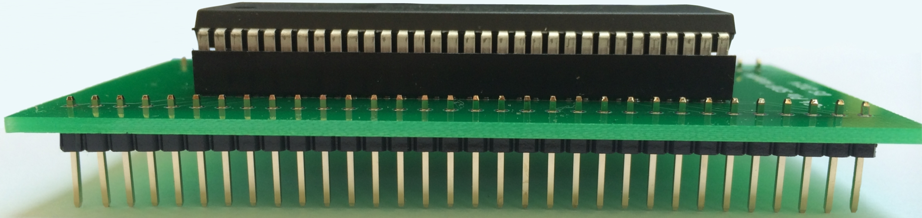
| Test fitting the socketed SDIP and 0.1" pitch
header pin strip to the bard board - everything
actually fits!
I'm quite relieved (surprised ?) as I had to
create the SDIP footprint myself - it is not in the
standard KiCad footprint library. |
 |
| Profile view - I may mount the headers on the
top side of the board to reduce the wasted space
below the adapter board, unless I use the space to
mount some passive components on the main board. |
 |
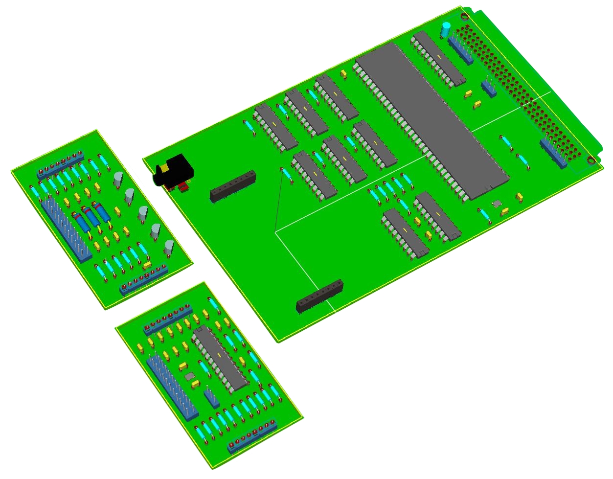
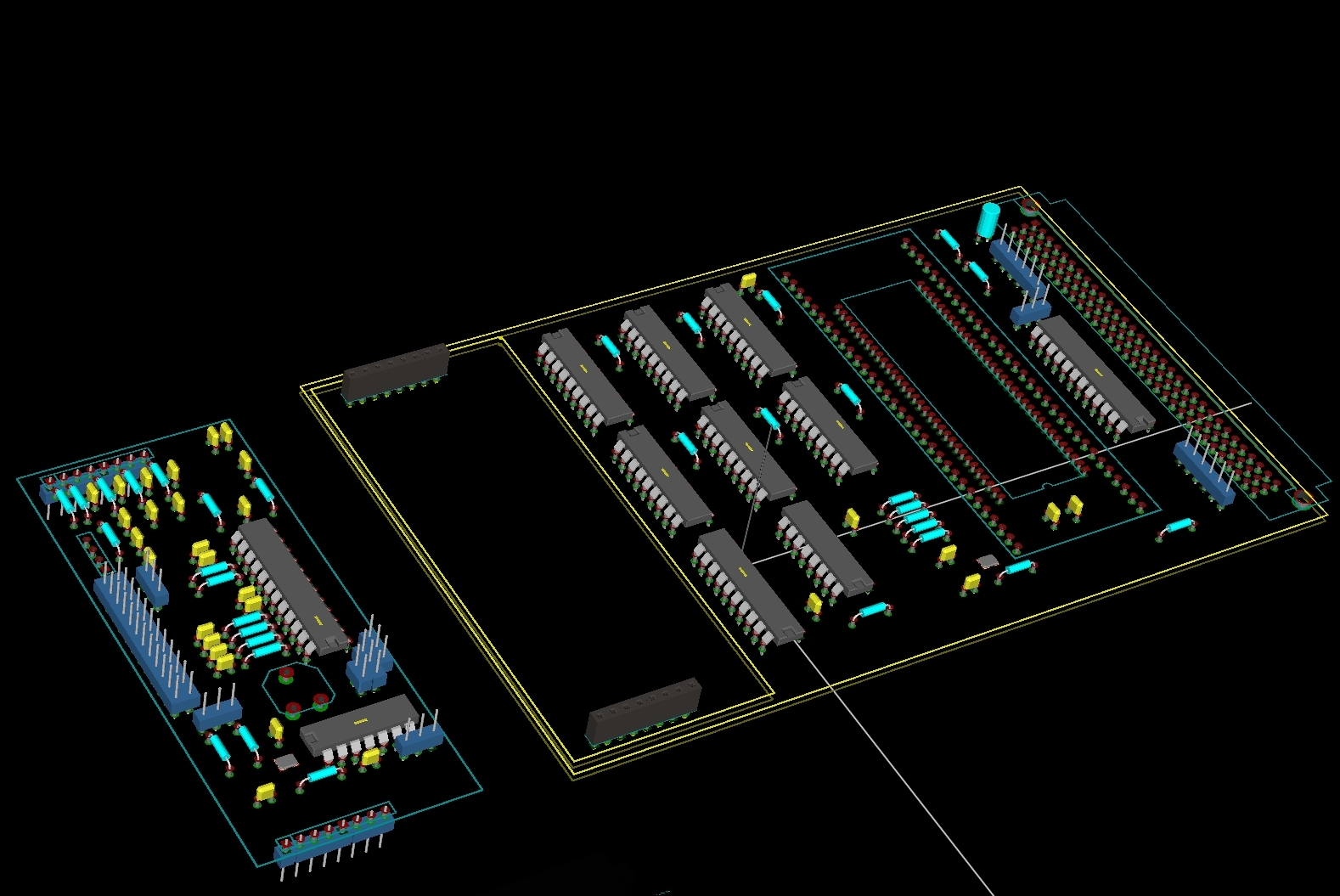
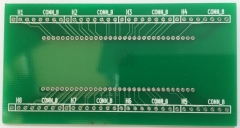
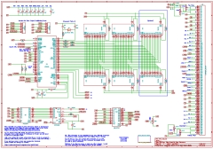
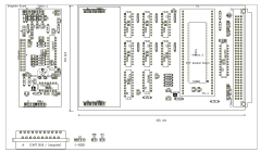
Board Design
| Draft version 0.6 of the video board design
The main board will accommodate the VDP, VRAM, sound
generator and the supporting chips.
The small daughter boards are for two different
signal conditioning boards for the audio and video
which will be cabled to the pin header at the left
hand side of the daughter boards |
 |
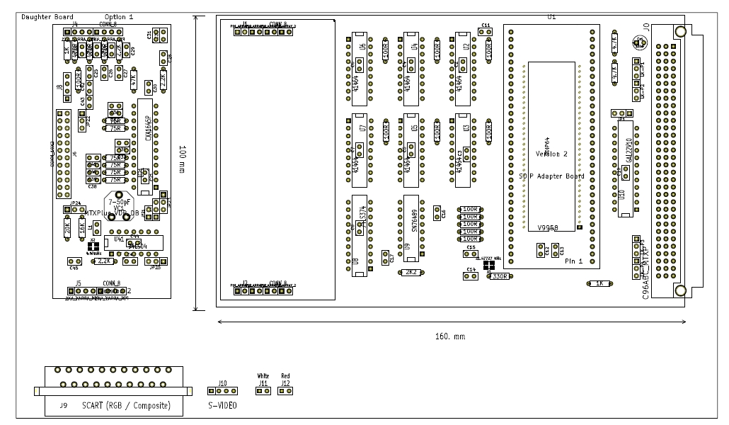
| This is Version 1.01 of the Video board design.
The "input" side of the board, including the RAM and
clock generation, is relatively straightforward, the
same basic design was used in computers in the MSX2
range (V9938) and the MSX2+ and Turbo R machines
(V9958).
The other chips on this page are the sound
generator, buffer and I/O decoder that will be
installed on the video board for convenience. |
 |
| The Video output from the VDP is a bit trickier
though, some V9938 machines used transistors to
amplify the RGB outputs and others used a Sony
CXA1445P RGB encoder. All MSX machines that had a
V9958 installed used the Sony encoder.
The CXA1445P is obsolete and difficult to find,
my design uses the later CXA1645P - which has more
video output options. It is just as obsolete, but
Lez has been able to source some for us. |
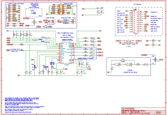 |
| Martin was a little uncomfortable using such
potentially hard to source decoders, so we decided
to make the video board flexible enough to cope with
a transistor based design as well as one using the
Sony encoder. The area at the left hand of the
main board has headers to allow an appropriate
daughter board to be installed. |
 |
| Although I have worked up a transistor based
design, because there needs to be some modifications
done to the transistor schematics used with a V9938
to work with a V9958, I am less confident of the
"analogue" design. At this point, we have parked the
analogue daughter board and will probably revisit
if/when the "digital" board has issues that we can't
resolve. |
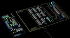 |
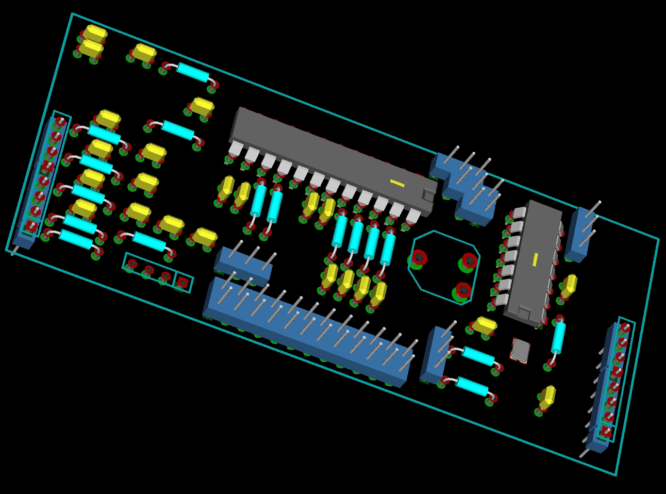
| A close up of the "digital" daughter board,
using a Sony CXA1645P. The other IC is a 74LS04
inverter package used for the optional PAL clock for
the encoder. The default output from the video
encoder is NTSC, the jumpers on the board allow PAL
to be selected - provided that the PAL clock
components are added. I am hoping that this won't be
needed as most modern TVs can handle NTSC as well as
PAL. |
 |
Firmware
The only firmware on the original video
board design described on this page was the GAL responsible
for I/O port decode and generation the "normal" VDP and PSG
control signals (MODE 0, MODE 1, VDPWR,
VDPRD,
IN3 &
OUT6).
The basic design of the video board proved
to be fine for operation of MTXPlus+ at speeds
comparable to MSX 2+ systems, but as the speed of the system
increased, the I/O devices, including the VDP, PSG and PIA,
were not able to keep up and software waits had to be added
to the ROM to allow the system to operate at higher speeds.
Whilst adding software waits to the ROM did
allow the system to run at higher speeds, these waits could
only be changed by rebuilding the ROM and configuring waits
suitable for operation at higher speeds meant that the speed
of operation at lower speeds was compromised by the
inclusion of additional waits that were not necessary at
lower speeds.
Tony Brewer devised a method of
automatically inserting hardware wait states as required
based on the system clock frequency, this functionality
required some modifications to the existing GAL and the
addition of a second GAL on the video board.
For details of MTXPlus+ firmware, including
the GAL fitted to the video board, see the MTXPlus+
firmware overview page.
References:
Roger
Samdal's Spectravideo site,
VDP page
GR8BIT project, Eugeny Brychkov,
GR8BIT Knowledge Base article on adding
Composite and S-Video output (KB0014).
|