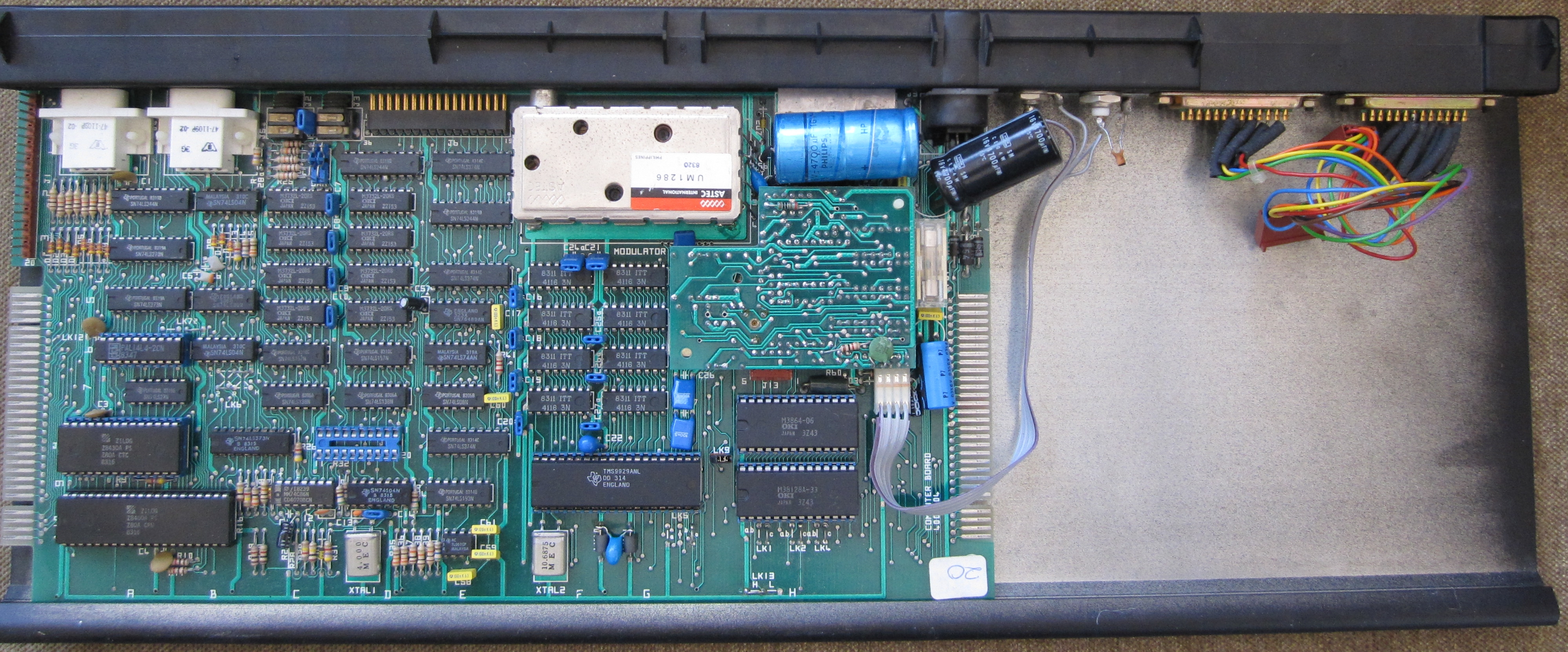
This page describes the process of
turning Martin's prototype design into a product that we can
make available for others to purchase - assuming that there is
interest of course.
I should mention at the outset, that one
my goals was to design something that, as well as being
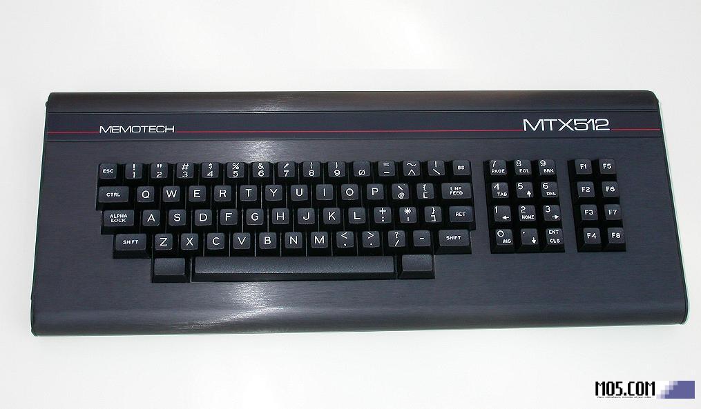
technically sound, also worked well aesthetically. The Memotech
MTX was one of the best, if not the best, looking of the many
home computers of the early 1980s and I think that hanging
devices off the end of it on the external connector really
detracts from its sleek lines.
At the outset, I decided that I
wanted something that would be mounted internally and any I/O
connections should be as unobtrusive as possible. This
inevitably means that the size of the board will be considerably
larger than is strictly necessary if only the electronic
components were to be mounted on it.
During
prototyping, Martin had confirmed that the FPGA
development board could be mounted onto a custom PCB to
interface to the MTX and fit below the MTX keyboard, but only if the PCB was level with
the MTX computer board.
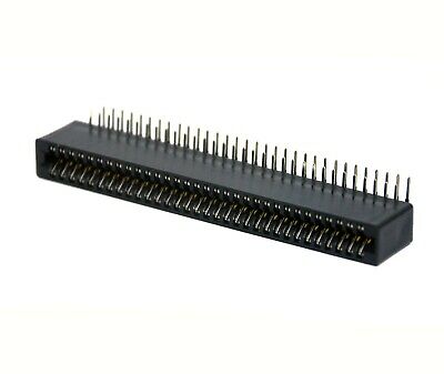
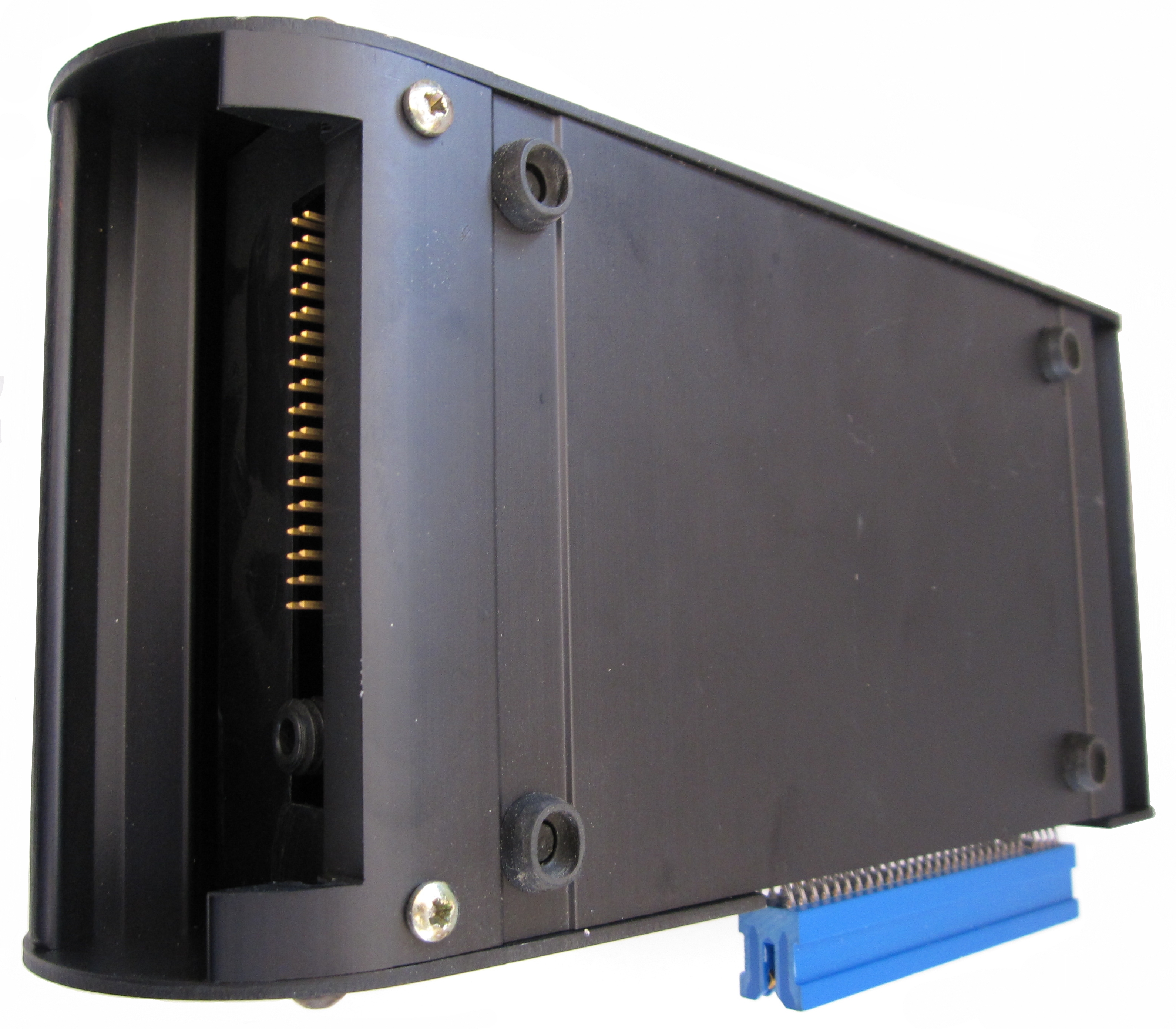
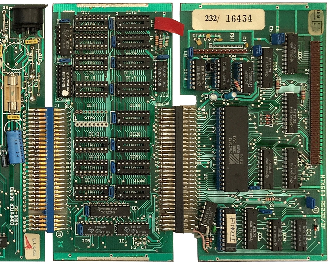
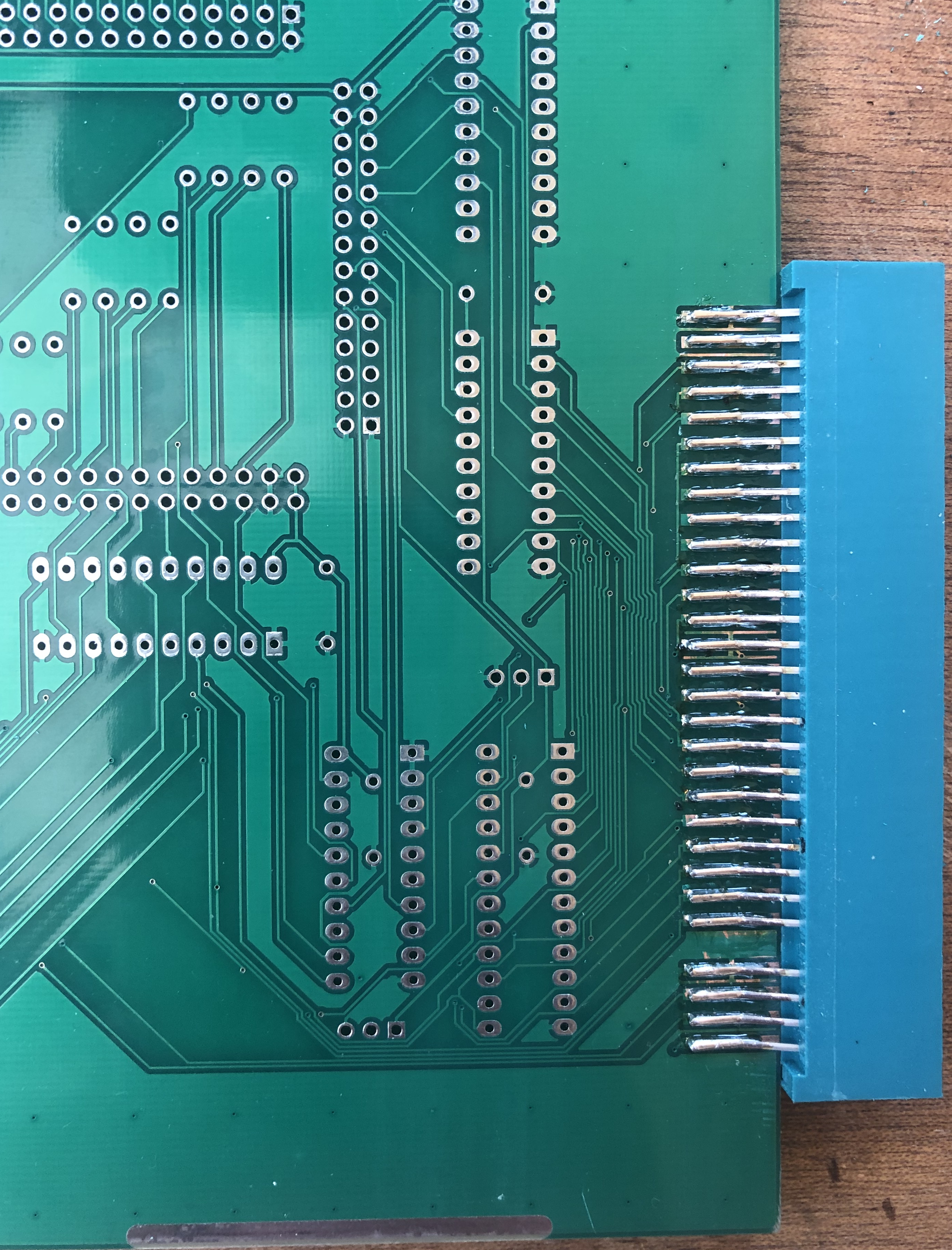
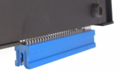
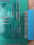
The edge connectors that
I have used for our previous MTX expansion boards are
right angled, which meant that the PCBs are at a
different level to the MTX computer board. |
 |
It also
worth mentioning the way that Memotech designed the
internal edge connector does not lend itself to
connection!
The PCB at both ends of the
connector is flush with the connector's edge. As you can
see from the edge connector photos, this means that the
ends of the connector must be modified to allow the
connector to fit over the edge of the board. |
 |
It's
not as if Memotech used a different type of connector
back in the day - all of Memotech's expansion cards had
their connectors modified to fit.
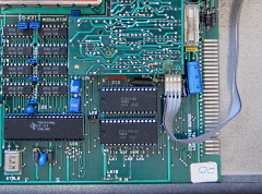
This close up
of the base of an SDX shows how Memotech sliced off the ends
of longer connectors to expose the opening between the
slots to allow the connector to slide over the PCB. |
 |
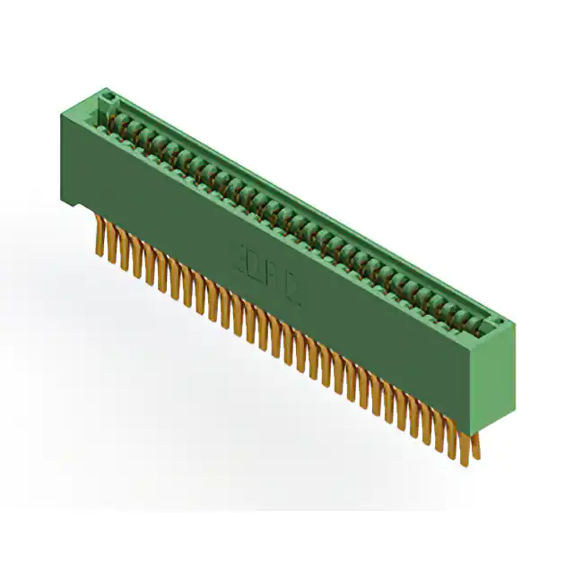
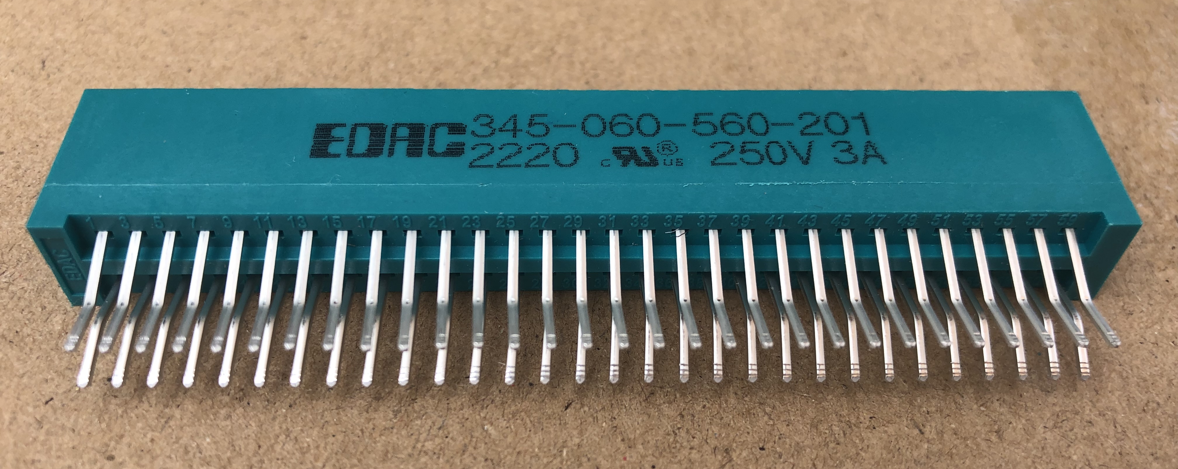
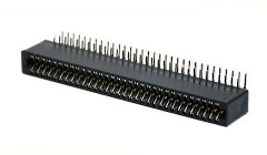
Straight
connectors similar to those used by Memotech on their
expansion boards are very rare these days. We did
identify a suitable connector made by
EDAC, but these are
"order on request" items with an 18 week lead time from
Digikey, along
with a minimum order quantity of 25 with a total price
of £150.
Once MFX looked like it would likely
fly, I decided to take a punt and order connectors,
rather than have to wait months once the design was
done. (I placed the order in April 2022, by July, the
price had more than doubled!) |
 |
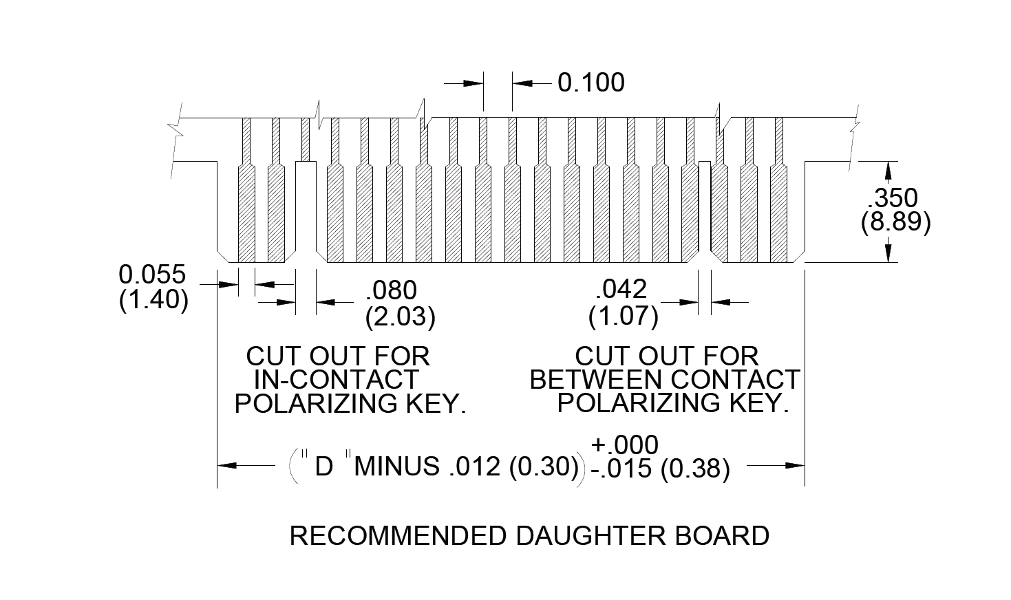
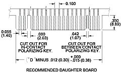
This
"recommended daughter board" drawing from the EDAC sheet
highlights where MTX made things difficult for
themselves - and for anyone developing modern day
add-ons for the MTX.
If they had left space to
attach the connector, it would have meant that
butchering the connector plug wasn't necessary. |
 |
On to the
board deign . . . .
All of the add-ons that I have built for
the Memotech MTX computer have been created using
KiCad, in its own words, "A
Cross Platform and Open Source Electronics Design Automation
Suite". MFX will continue that journey . . .
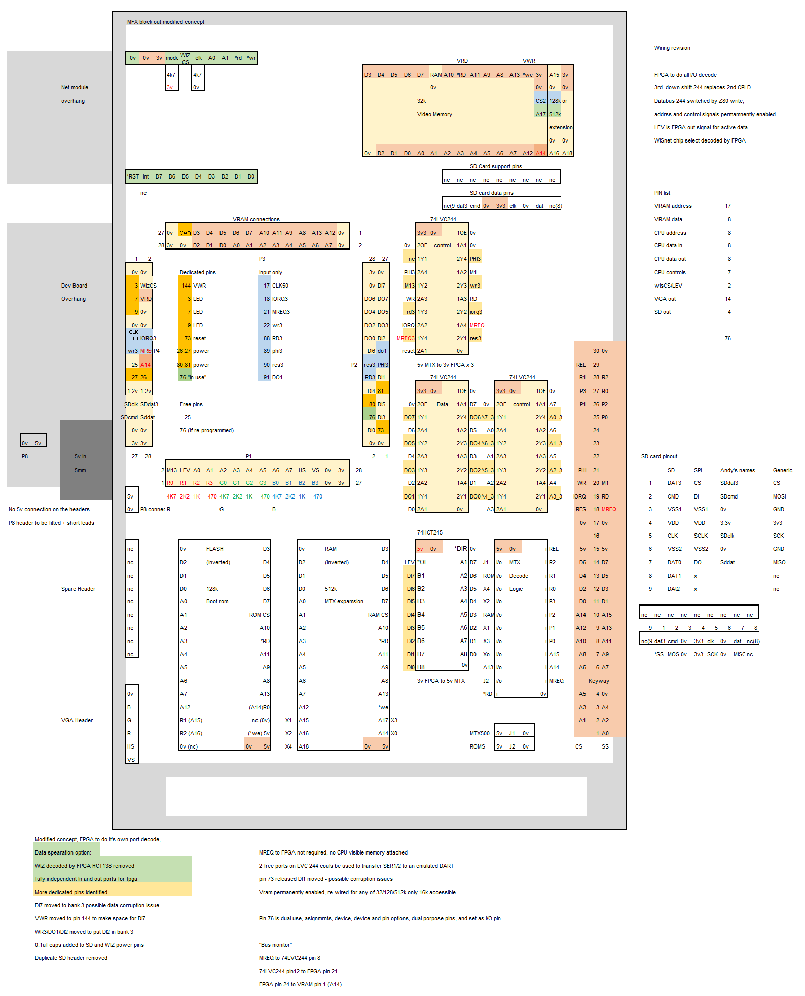
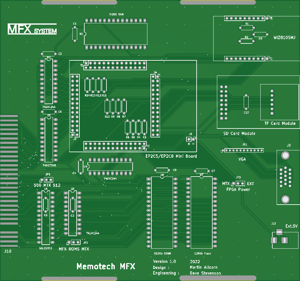
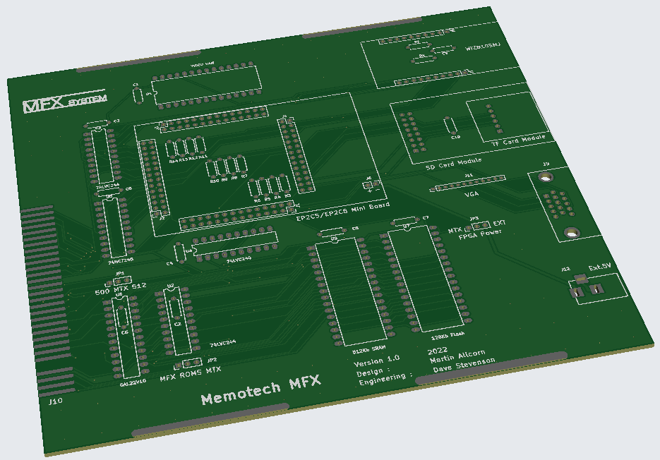
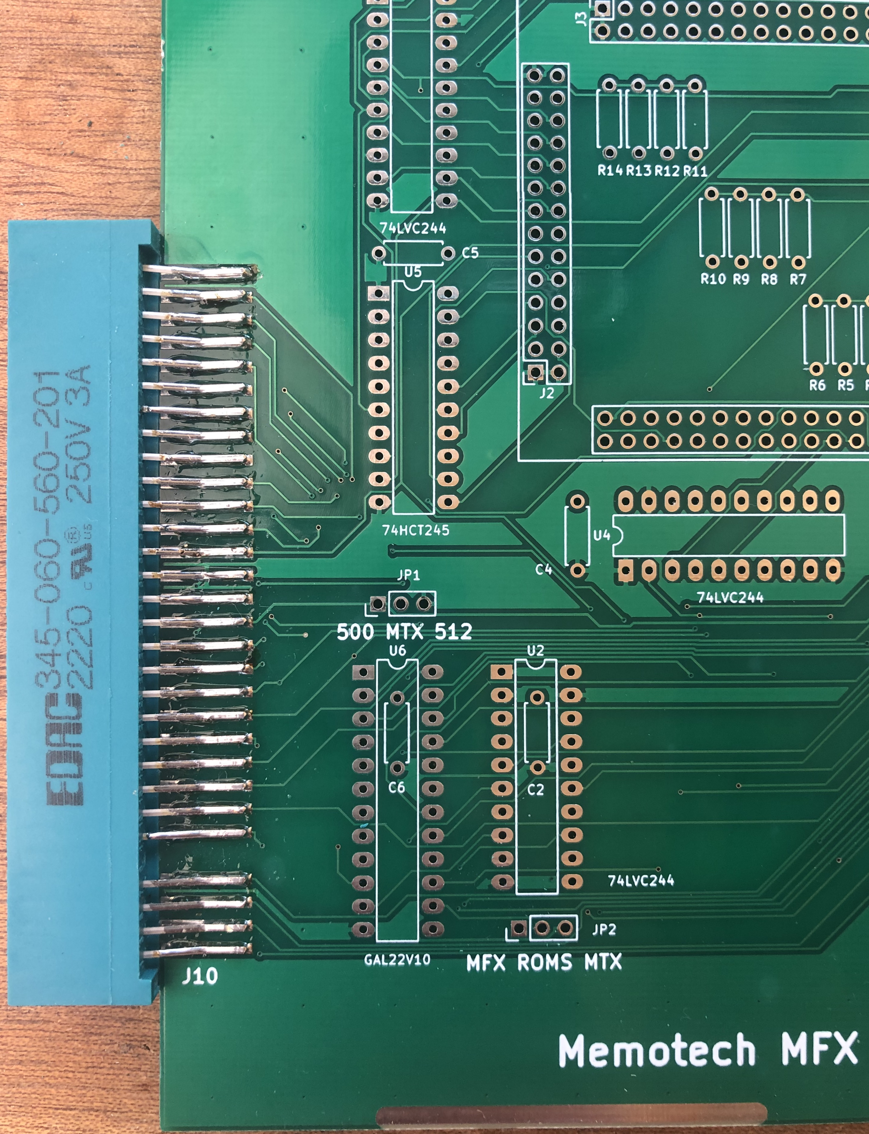
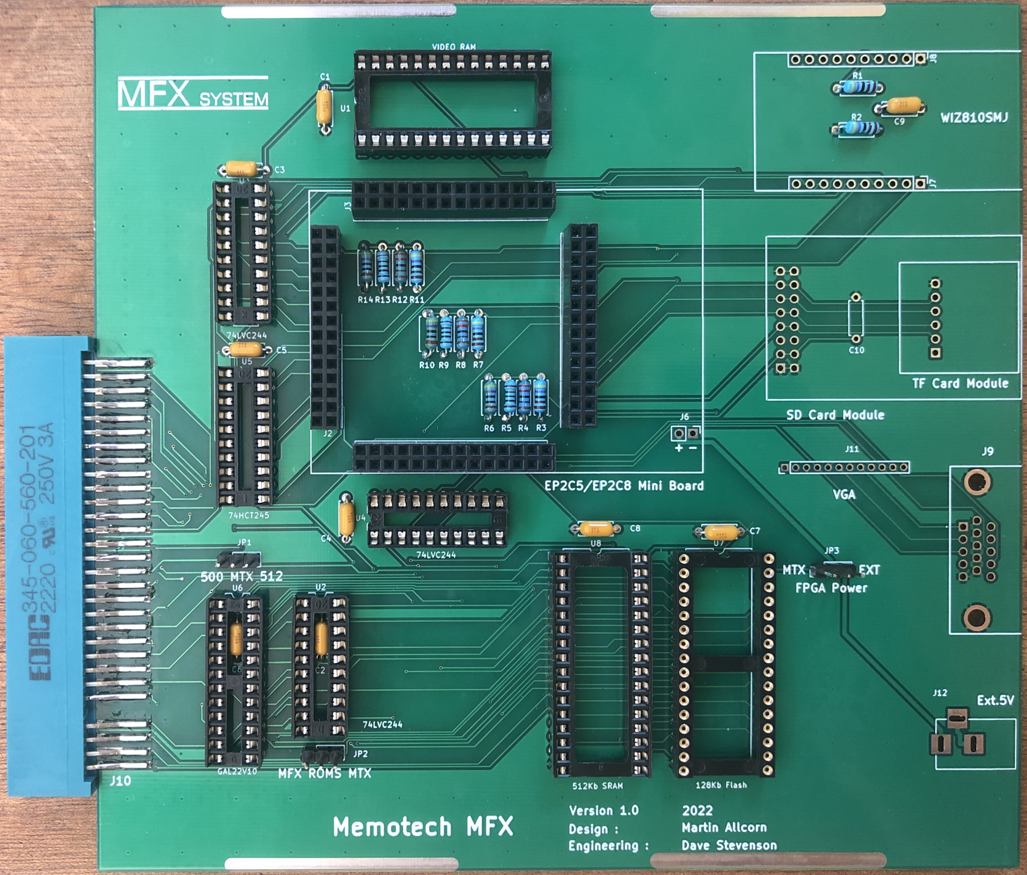
In
addition to the FPGA and I/O connections, the board has:
512kB SRAM for MTX RAM expansion
128kB Flash for ROM images
32kB SRAM for VDP
shadow RAM for the VGA output
GAL22V10 for
memory address decoding
74HCT245 for level
shifting between FPGA and MTX
3 x 74LVC244 for
level shifting between MTX and FPGA
WIZ810 network module |
 |
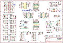
The first step is to take Martin's
"blocking" diagram and create a "proper" circuit diagram using
KiCad's schematic editor.
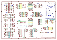
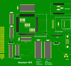
The first rev of the schematic |
 |
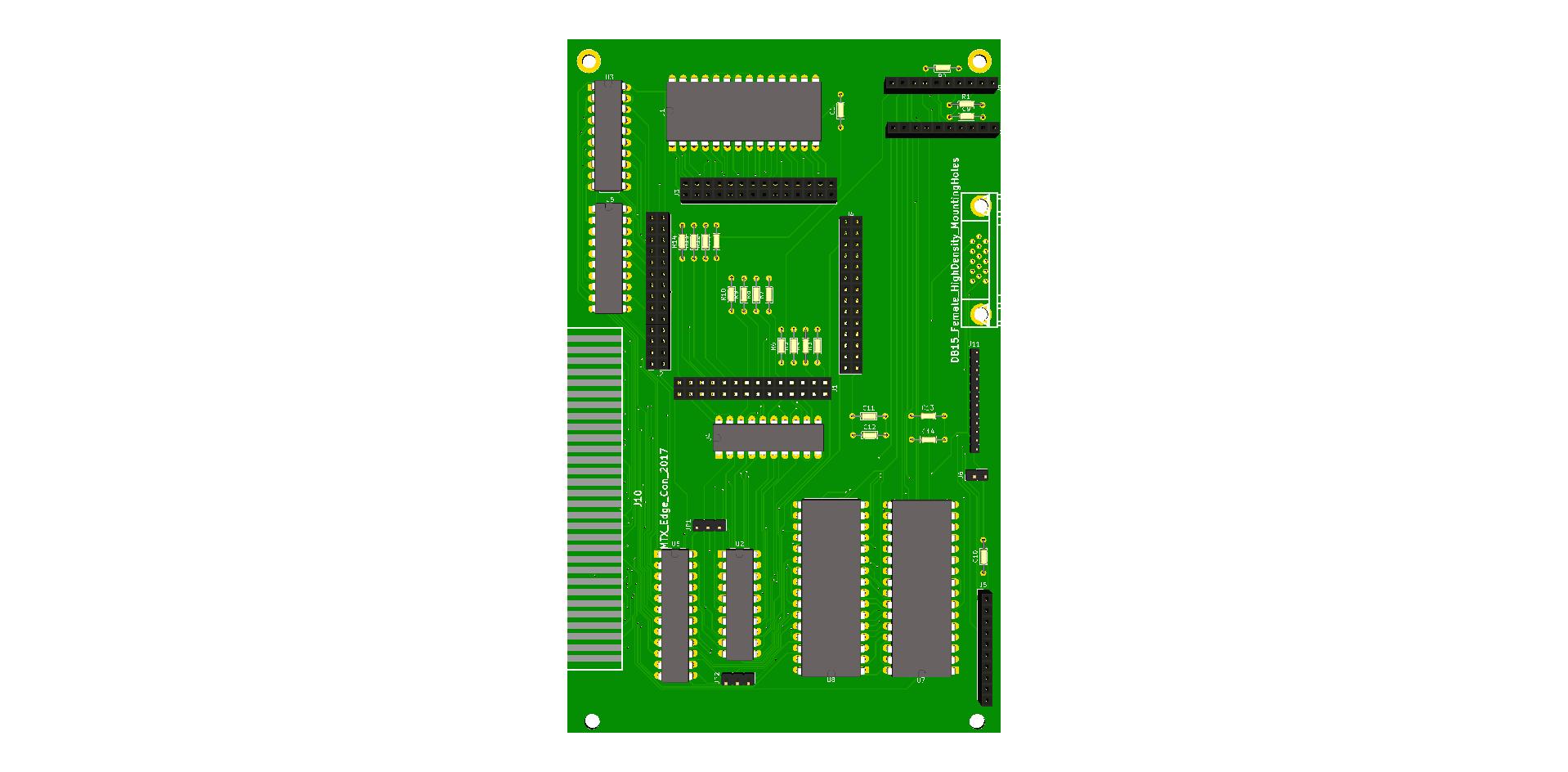
Once the
schematic has been "finalised" and checked for any
errors, footprints are assigned to the components and
board is designed using KiCad's PCB designer.
The tool has an automatic component placement feature,
but I find that it takes ages to run and get better
results when I manually place the components, taking
into account the main connections between them. |
 |
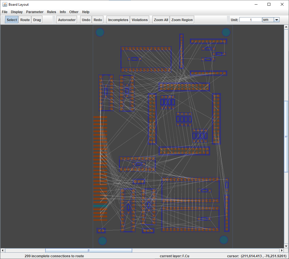
I use an
older version of the
FreeRouting tool created by Alfons Wirtz. Currently,
I run it as a standalone Java application, but will
upgrade to the latest version soon.
The
Autorouter tries to route signals it finds in the KiCad
netlist and, if successful, goes on to optimise the
solution, which reduces the number of
vias in the board. |
 |
I find
that it is an iterative process - I probably never get
to an optimal solution, but I can usually quickly see
where improvements can be made and move things around
accordingly until I get to something that I am happy
with.
Spot the difference ? (Here, I have moved a
couple of the level shifters around and removed the
board mounted VGA connector) |
 |
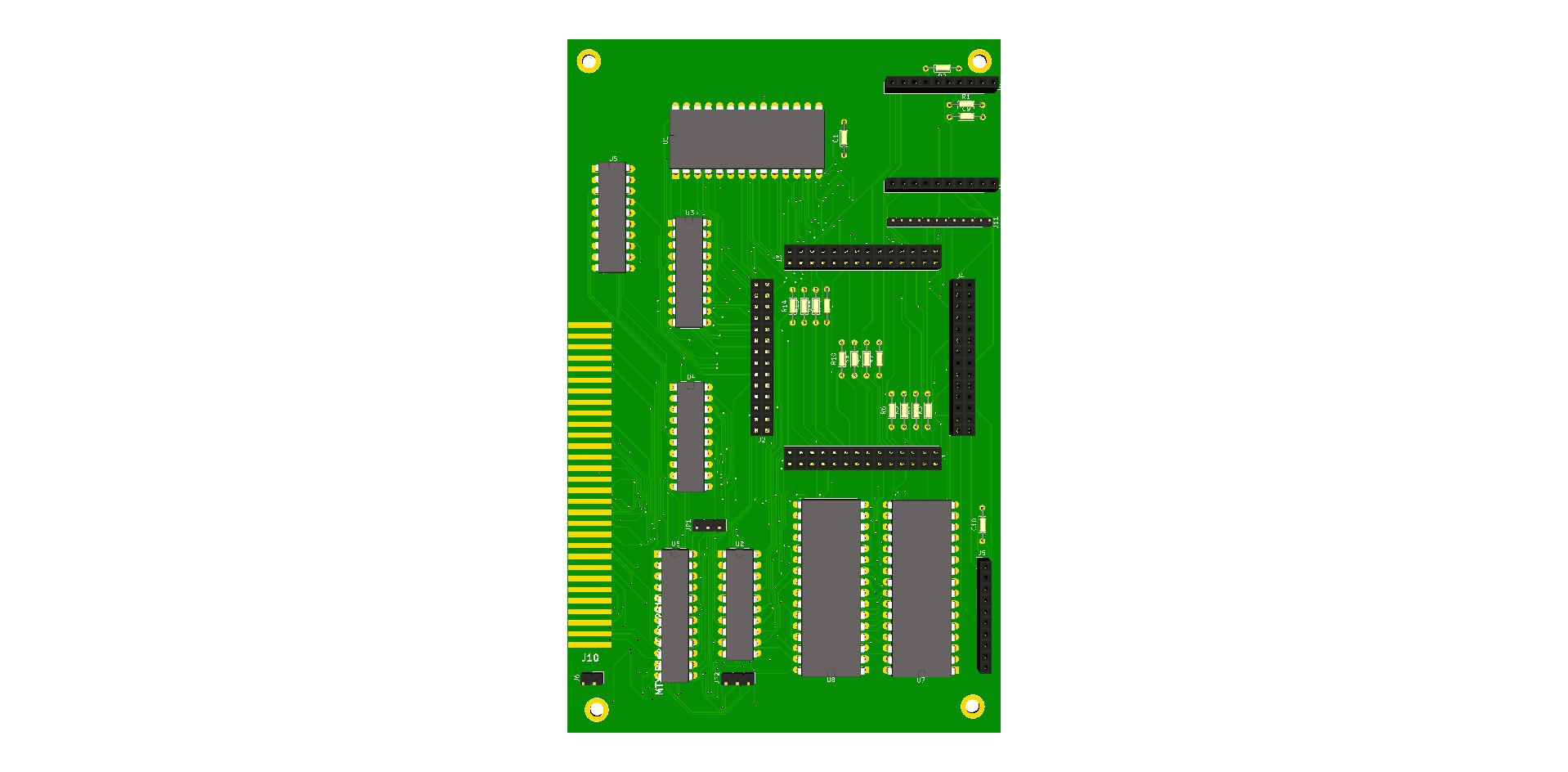
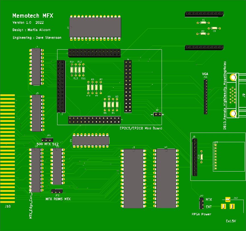
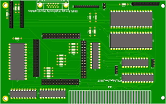
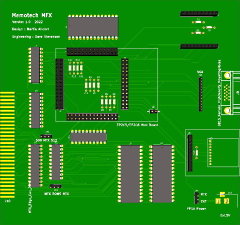
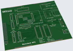
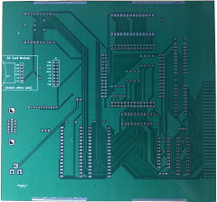
This
layout is Eurocard sized (160mm x 100mm) and has headers
for the WIZ810, SD card module and VGA connector. It
pretty much meets our initial aspirations regarding
board size.
Mated to an MTX computer board, it
would sit about 70mm away from the right hand end plate,
meaning that wiring to end plate mounted I/O connectors
would require internal cables. It would be possible to
run cables for the network and VGA monitor out through
the rear of the MTX case, but this would be rather messy
and short adapter/extension cables would add some cost.
Martin and I had some discussion on the best way of
facilitating connection to the PCB and decided that a
slight change of approach was needed. Rather than
minimising the PCB footprint (and cost), since any extra
space inside the MTX would be pretty much wasted, it
made more sense to dispense with the need for cables and
make the PCB wide enough to reach the end plate. This
would end up with a PCB of similar size to Memotech's
internal 80 column board, slightly increasing the cost,
but this would be more than offset by the savings made
by not requiring additional cables. |
 |
For
comparison, here is a photo of the Memotech internal 80
column card, used for the SDX CP/M video output. You can
see the connectors for RGB and composite video, as well
as a hole for an external power supply (which was not
used unless the 80 column card had the DART option
installed).
We had toyed with the idea of
including a second bus connector to allow MFX to be
connected externally, but despite the larger sized PCB
having ample space, having a board this size
hanging off the end of the MTX is silly, so the idea was
dropped. |
 |
| For
development, Martin's FPGA board was powered from an
external DC PSU. Since MTXs and/or their PSUs can have
some variability in their power characteristics, we
checked how Martin's system performed when the FPGA was
powered from the MTX. This resulted in a small amount of
"wobble" on the VDP AV output. This may be unique to
Martin's MTX, but provision for an external 5VDC supply
was added to the PCB design. |
 |
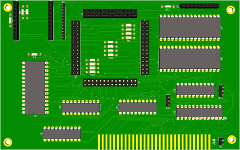
Draft
layout of a square, rather than rectangular, board.
Although there appears to be a large amount of
wasted spaced, a design such as this would allow direct
connection of the I/O through the right hand end plate.
An added benefit is that there is no need to place
components where the MTX audio and video connectors are
on the rear panel.
The fixed VGA connector has
been reinstated, along with a barrel jack for an
(optional) external 5VDC power supply. |
 |
| Martin
suggested that the VGA connector could be made
accessible through the RS232 port cut-out and 3D printed
a possible insert to fill the cut-out. Unfortunately
many VGA cables are too bulky to fit into the RS232
recess. We considered a couple of ways that this might
be made to work, but decided that end plate access was
definitely the way to go. |
 |
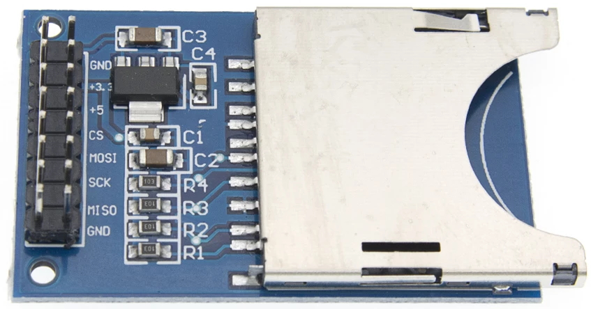
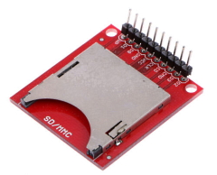
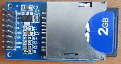
I spent
quite a bit of time trying to decide what type of SD
card module I was going to use, whether full size or
TF sized; whether bare board or something more complex?
Martin had used a bare SD slot in his prototype, the
only addition being a bypass capacitor for the power
supply to it. Breakout boards like this are quite common
and have a footprint not much bigger than the SD card
slot itself. However, many SD modules have quite a few
passives fitted and I wasn't sure why. |
 |
| Andy had
used a board like this for REMEMORizer. The SMT
components are a voltage regulator, a few resistors and
a few capacitors. |
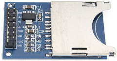 |
The
voltage regulator is there to allow the 3V SD card to be
interfaced with 5v devices (this version has no level shifting
on the data lines though.)
In this image of
the circuit diagram, you can see that resistors are used
to pull the SD card data lines up to 3.3V. I was not
able to find a definitive answer on the web as to
whether these are required or not.
Martin's
system obviously worked without them and from what I
have been able to find, it is not an
SPI requirement. It seems that some SD card
manufacturers specified pull-ups for their SD cards. It
may be that some older SD cards need them, but newer
ones do not and many SD cards seem to have weak internal
pull-ups in the card. In any event, I think it safer to include
them than not, so I will be making sure that the PCB can
cater for this, larger sized, type of module. |
 |
| A very
small number of the Chinese suppliers of these modules
ship them without the header pins attached, but the
majority fit the headers to the top of the PCB. So as
not to restrict the number of sources of these module, I
will use the more common ones with the headers
preinstalled. This means that the SD card module will
need to be mounted on the MFX PCB upside down - as Andy
did with REMEMORizer. |
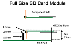 |
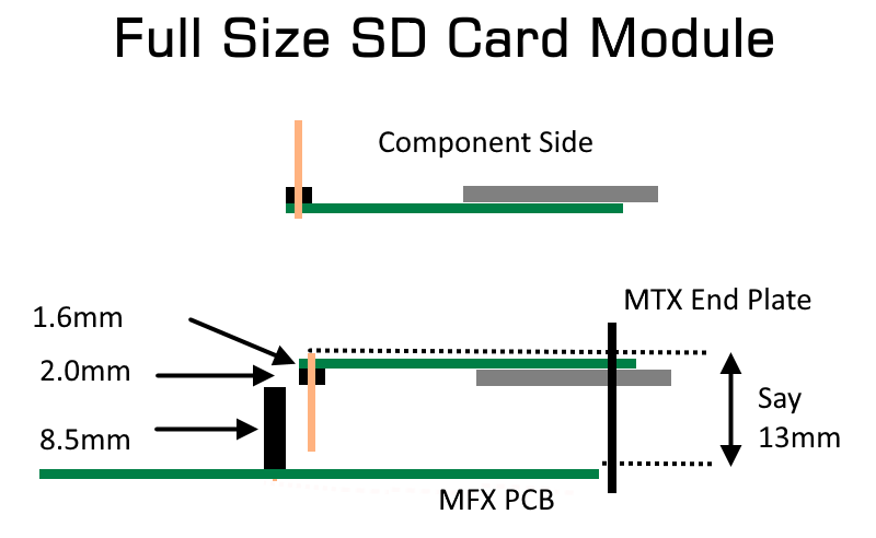
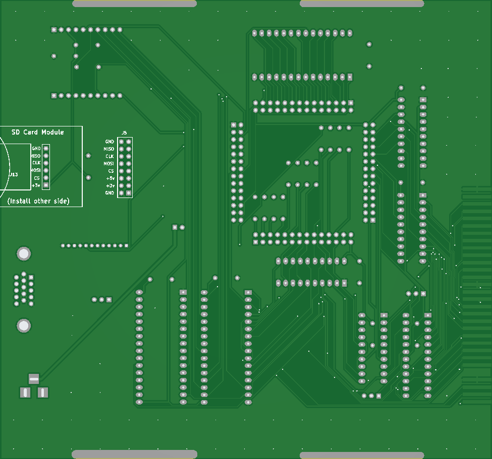
The SD
card modules with components on them are relatively long, at around 35mm, which
means that if the module is not to be permanently
soldered to the PCB, a header socket on the PCB needs to
be some distance from the right hand edge of the PCB.
The restricted clearance below the MTX keyboard PCB
means that there is not enough headroom to mount an SD
card module as it is shown in this first drafts for the
larger PCB. |
 |
To get
clearance for the SD card module, it was necessary to
swap the positions of the VGA connector and SD card
module. The VGA connector can easily fit in the shallow
part of the case as the keyboard PCB stops some 30mm
short of the right hand end of the case. Moving the VGA
connector closer to the front edge of the MTX end plate
was not ideal, but appeared to be the best option.
With the components and I/O connectors placed, I
felt that I was pretty close to getting a trial run of
boards made. However, whilst this was not going to be a
first for me, I am still a novice at this stuff and was
sure there was lots of scope for improvement. |
 |
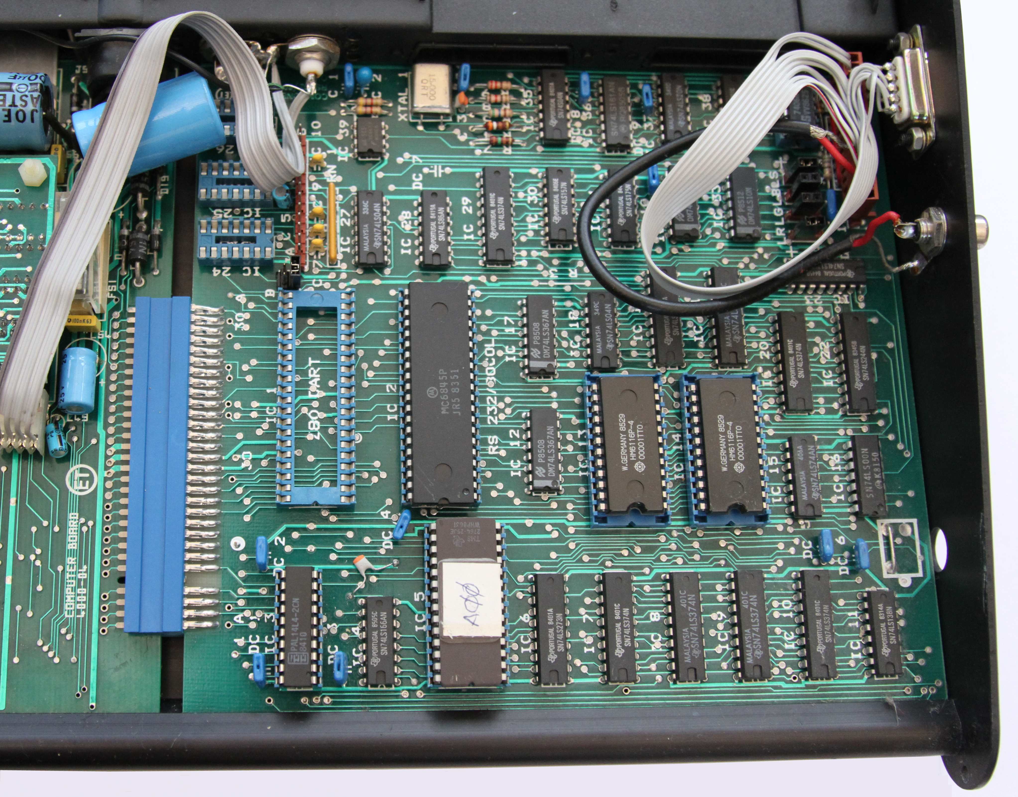
You can
see in this photo of a MTX RAM card and an RS232 board,
that although Memotech did not have ground planes, the
expansion boards have large ground strips at the top and
bottom of the board.
There are "holes" in the
solder mask on these strips to allow the ground to
contact the case metal work. Memotech were not
consistent in their use - neither the MTX computer board
or the 80 column board had these strips. |
 |
Many of
the 2-layer hobbyist PCBs that I have seen include
ground and/or power planes on the top/bottom of the
board. I think that this helps with noise reduction,
particularly for boards that operate at much higher
frequencies than the MTX. It appears that good design
practice is to have at least a ground plane on one or
both sides of the board - this has been added here.
There is not 100% coverage, but additional VIAs have
been added to fill the major void spaces left by the
auto-fill algorithm in KiCad. I also removed areas of
the solder mask at the board edges to allow the ground
to contact the case - though I'm sure they'll be of no
benefit here. |
 |
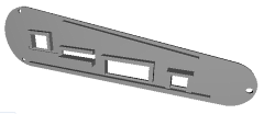
| This
mock up shows how a 3D printed end plate might look with
apertures for the I/O connectors placed to suit the PCB
above. |
 |
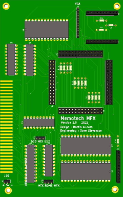
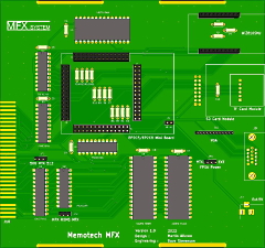
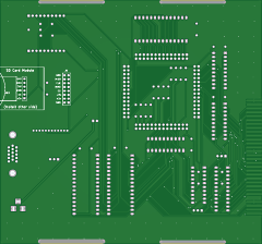
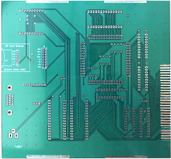
| "Final"
version of the PCB design, reflecting the changes shown
on the rendered image above |
 |
OK, first
draft done - including needless complications such as
ground planes and solder mask voids as described above.
Now I just need to bite the bullet and submit an order
for PCBs, then a few weeks later - find out how many
mistakes I've made along the way!
I will likely
wait until I have a definite shipment date for the EDAC
connectors and have gathered together more of the
components that I'll need before I "push the button" on
the board's manufacture, so there is still a little time
for "tinkering".
|
Here we go
!
I tried pricing up the board with the PCB
manufacturer that I usually use, but found them to be
quite expensive for this size of PCB. There are a number
of different Chinese PCB manufactures that cater for
hobbyist projects, and by shopping around a did find
that most were cheaper.
Time will tell if the
one that I chose has the quality of my previous
supplier, but I wanted to minimise costs until I had a
proven design. |
 |
This
supplier also has a neat on-line visualisation tool -
here is their representation of the PCB. Now I just need
to wait for delivery !
Damn !
Whilst I way
playing with the online viewer, I realised that I had
made an obvious mistake and the boards would have at
least 1 issue |
 |
Can
you see the problem ? . . . . . . .
Looking at
the reverse side of the board, you can see that the
solder mask layer (grey) is missing on the edge
connector pads :-(
When I cloned the pads on the
footprint's component side for the solder side, I didn't
change the mask layer from front to back! It will be
difficult to remove the mask from the pads, but we'll
see if it can be done when I get the boards.
But
I am not optimistic . . . . |
 |
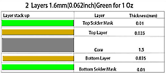
| This
image, from
pcbgogo.com shows the structure of a typical 1.6mm
PCB like the one ordered. The copper layers are "1 oz"
thick, equivalent to 35um, 1.4 mils or 0.035mm! There
won't be much copper to play with when I try to remove
the solder mask. |
 |
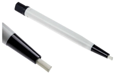
By design,
the solder mask layers are difficult to remove, it can
be done using some quite harsh chemicals, but I have
read that good results can be achieved by mechanical
means, i.e., scraping, using, for example, a fibreglass
brush such as this
one from RS.
I have one of these in my
toolbox; they need to be used with care as they shed
tiny shards of fibreglass which can cause irritation and
pierce the skin, but this is what I am planning to try. |
 |
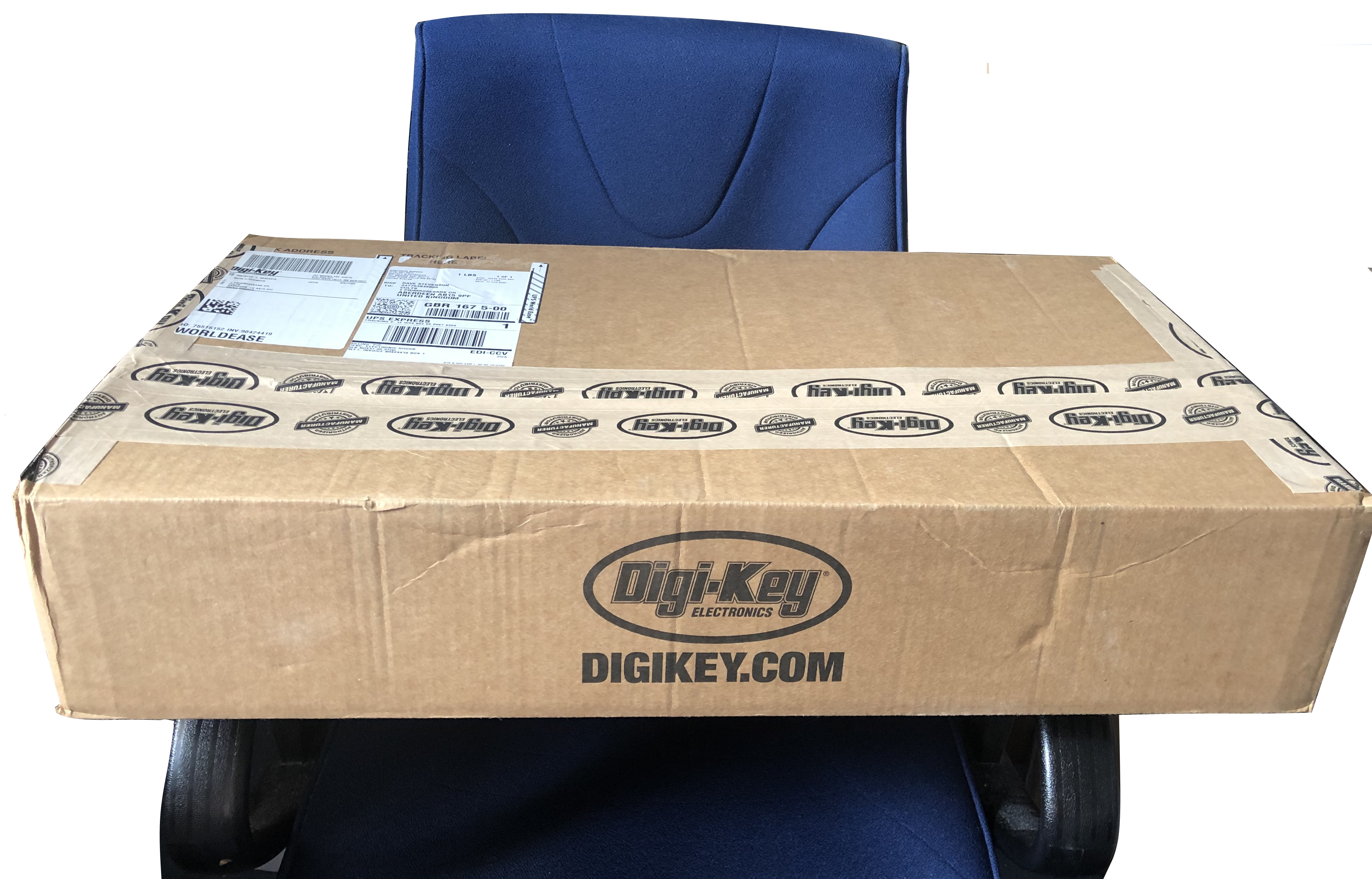
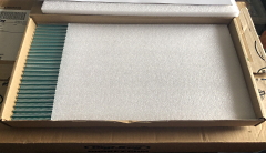
In the
meantime, the EDAC connectors from Digi-key arrived -
some 4 weeks ahead of the projected delivery date.
The size of the package took me somewhat by
surprise!
To show scale, here's a photo of the
box on my computer chair - the only contents were the 25
edge connectors that I had ordered! |
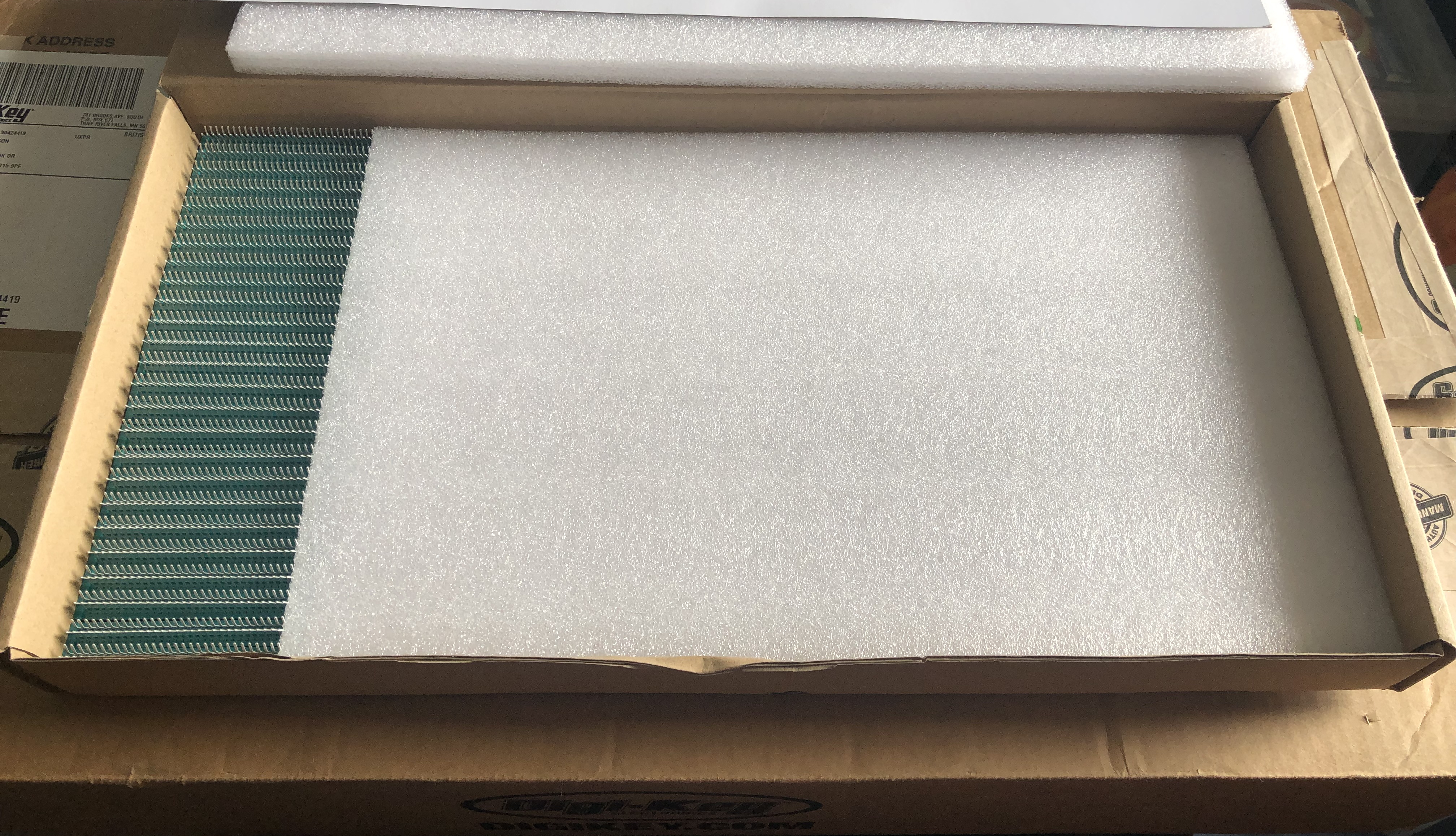
 |
| The EDAC
shipping carton looked like it was designed to hold 300
connectors in two layers of 150 each. It appears that
they don't expect smaller order quantities such as mine. |
 |
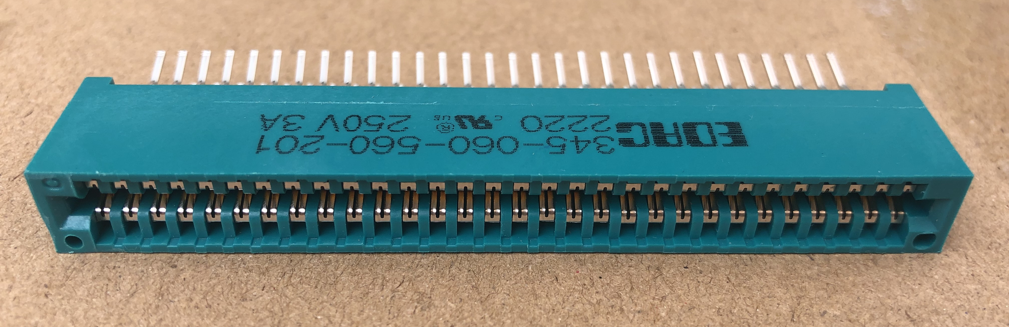
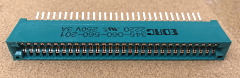
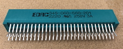
Front and
rear view of the connectors.
The datasheet
advises that the contact material is copper alloy with
"Gold Plating on mating area and Tin Plating on tails
with Nickel underplating all over". |
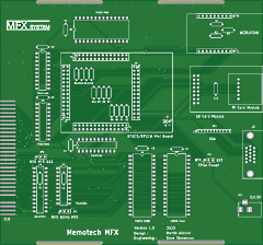
 |
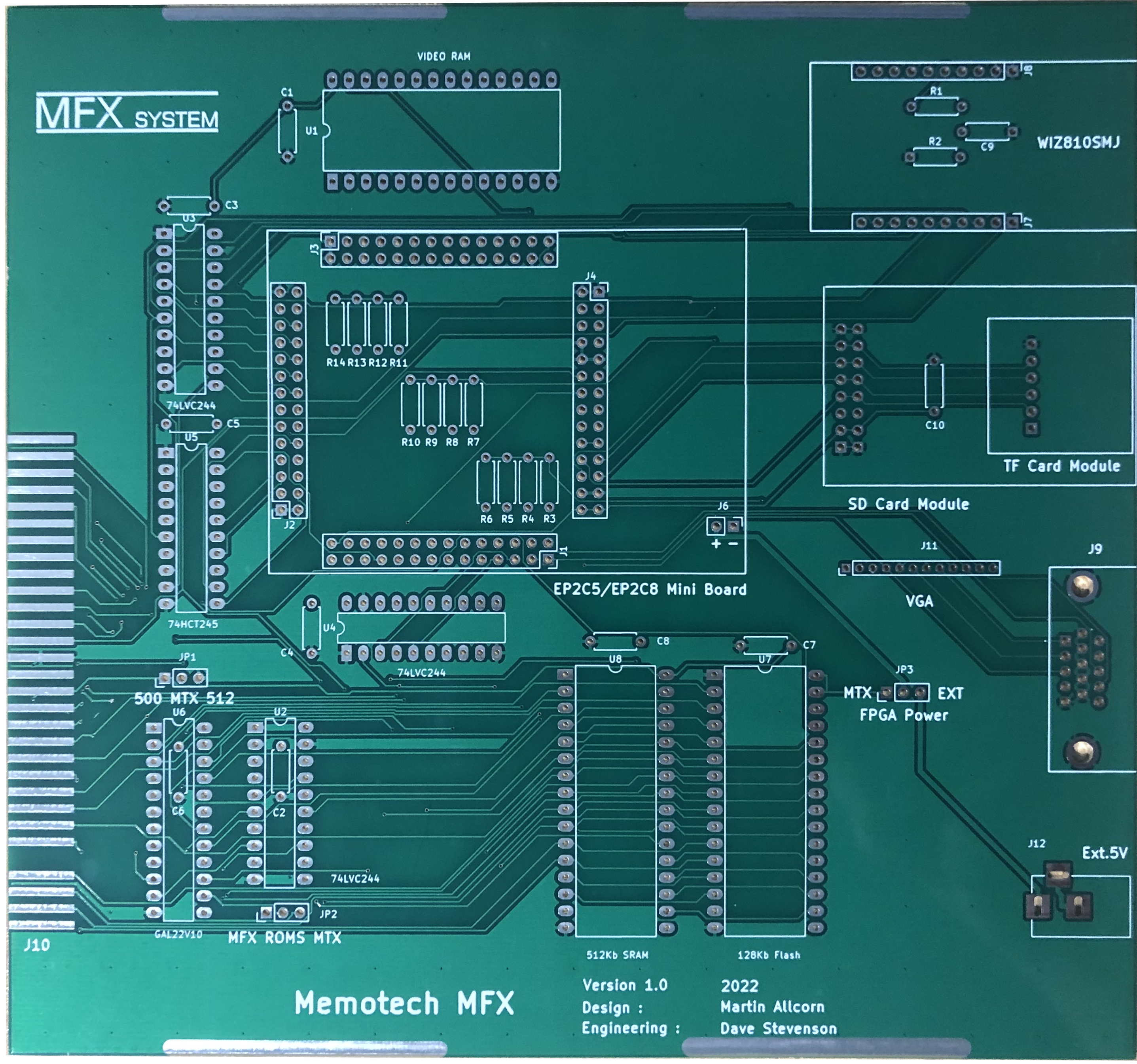
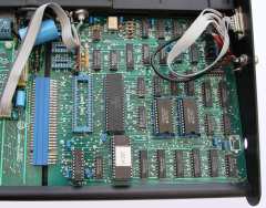
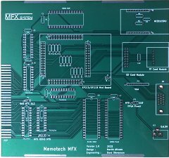
The PCBs
have arrived
Component side of the board.
It looks OK and some brief electrical checks were
fine, but I need to check positions of the components -
particularly the alignment of the headers for the FPGA
module. |
 |
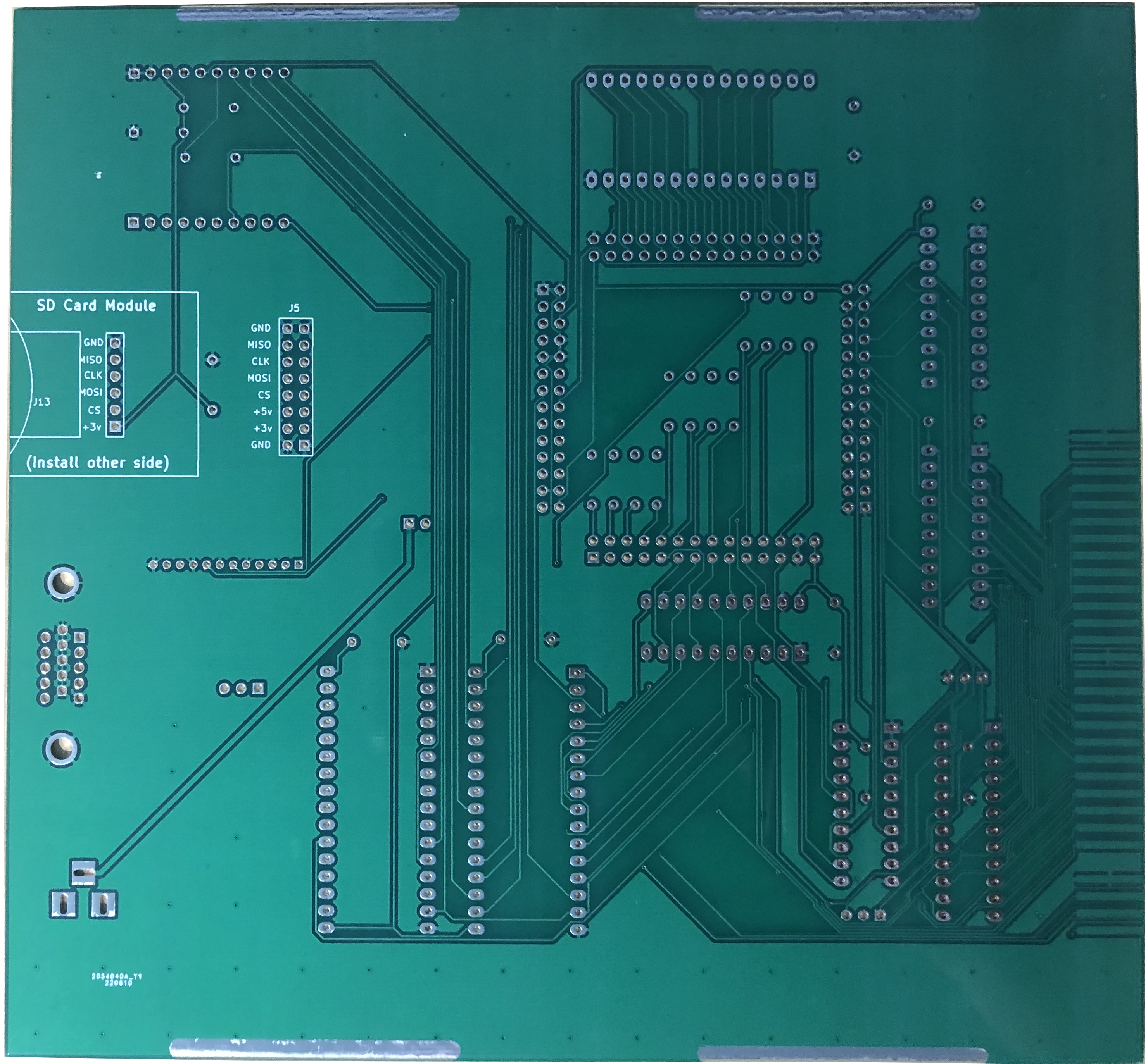
Solder
side of the board.
With the solder mask coating
the edge connector fingers as described earlier shown. |
 |
I managed
to removed the solder mask from the edge connector, but
found that the fibreglass brush struggled to get through
the coating.
I used a new Stanley knife blade,
removed from the knife and scraped off the coating,
using the flat of the blade, trying to avoid digging the
point into the copper trace.
The KiCad ground
plane fill had placed some narrow ground zones between a
couple of the fingers and I was a little worried that
removal of the solder mask might make it hard to solder
the connector without creating bridges to these areas. |
 |
| I did
consider scraping off these thin areas of ground plane
between the fingers, but decided not to. The close up
photo shows some small remnants of mask that shouldn't
be an issue, I didn't want to go too far and damage the
thin copper, but it was actually much more robust than I
had expected. |
 |
Edge
connector soldered to the board. Even with the exposed
areas of ground plane between the fingers, I managed to
fit the connector without creating any solder bridges.
The board would look better without the EDAC label
being so prominent - next time I will mount the
connector with the EDAC label on the bottom. |
  |
The
headers for the FPGA seemed to be in the right place,
there was nothing else obviously wrong, so I made a
start on assembling the board.
I was still
waiting for some items to be delivered, mainly the SD
card modules, so there was not much further I could go
until they arrived. |
 |
However, I
could at least test that the ROM was booting and the RAM
expansion was working.
ROM, RAM and PAL installed
with the MFX PCB pinned for a MTX500 where the PCB was
installed.
At this point, you can see probably
the largest (by area) memory only upgrade board ever
installed in an MTX ! |
 |
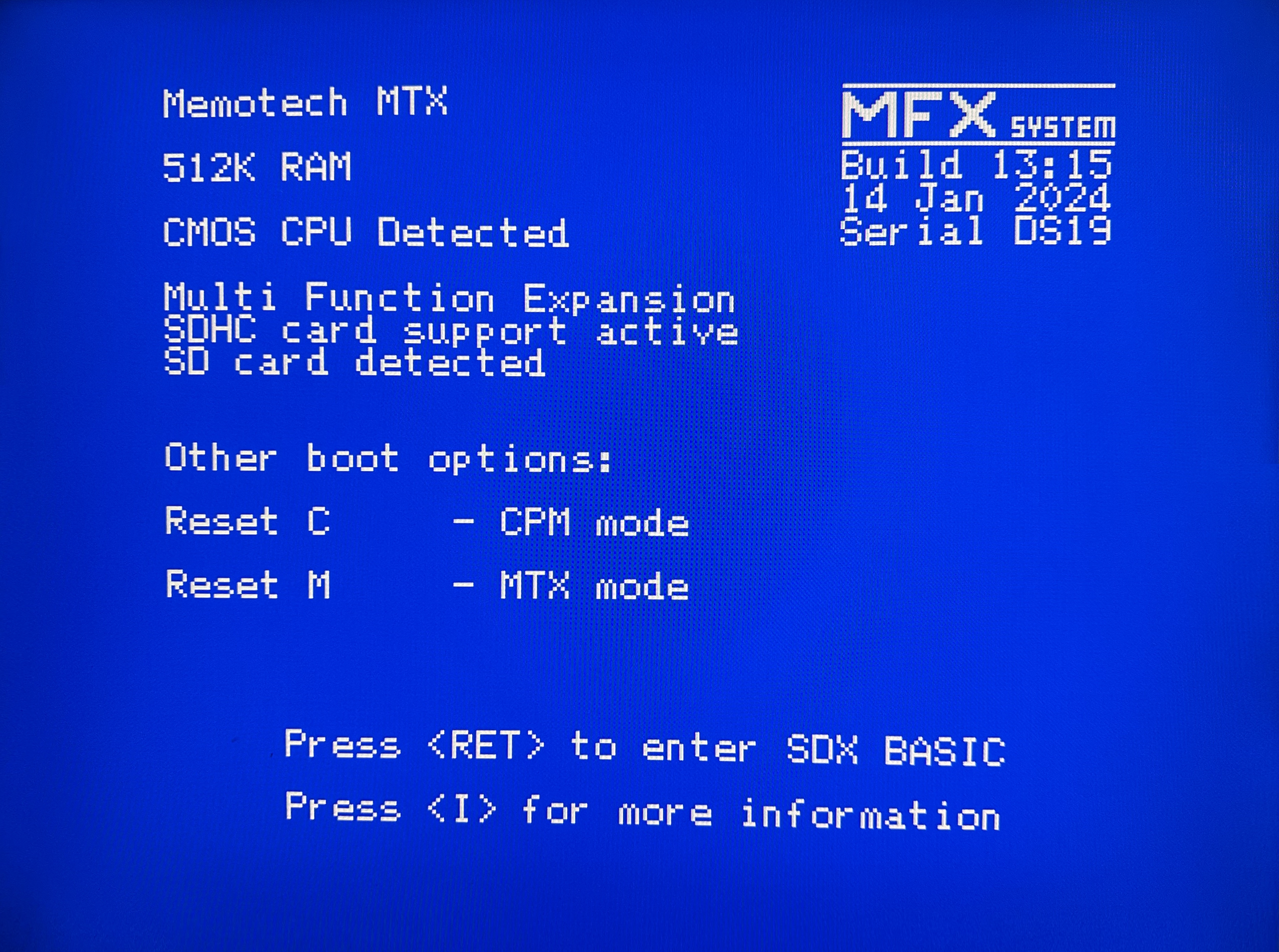
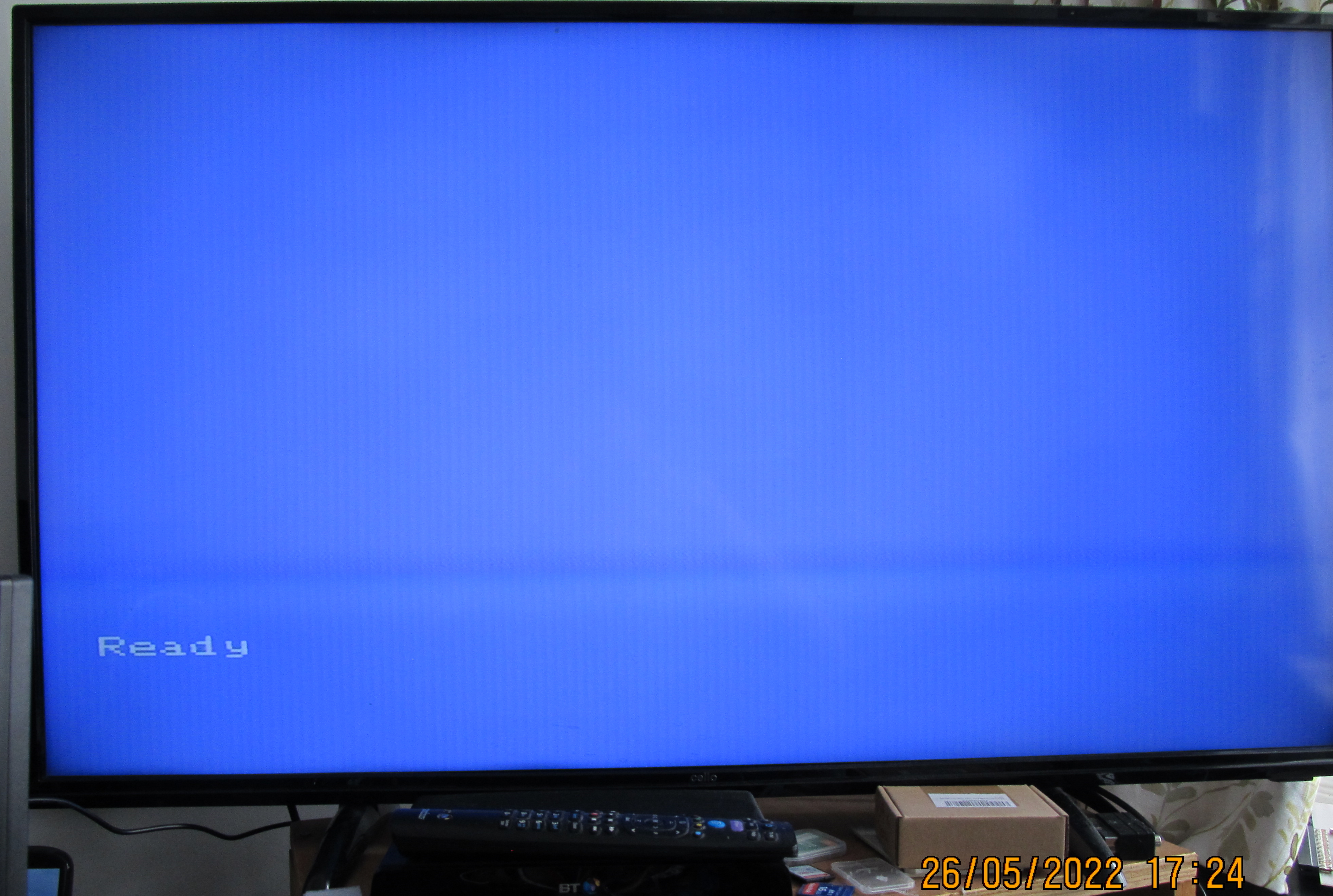
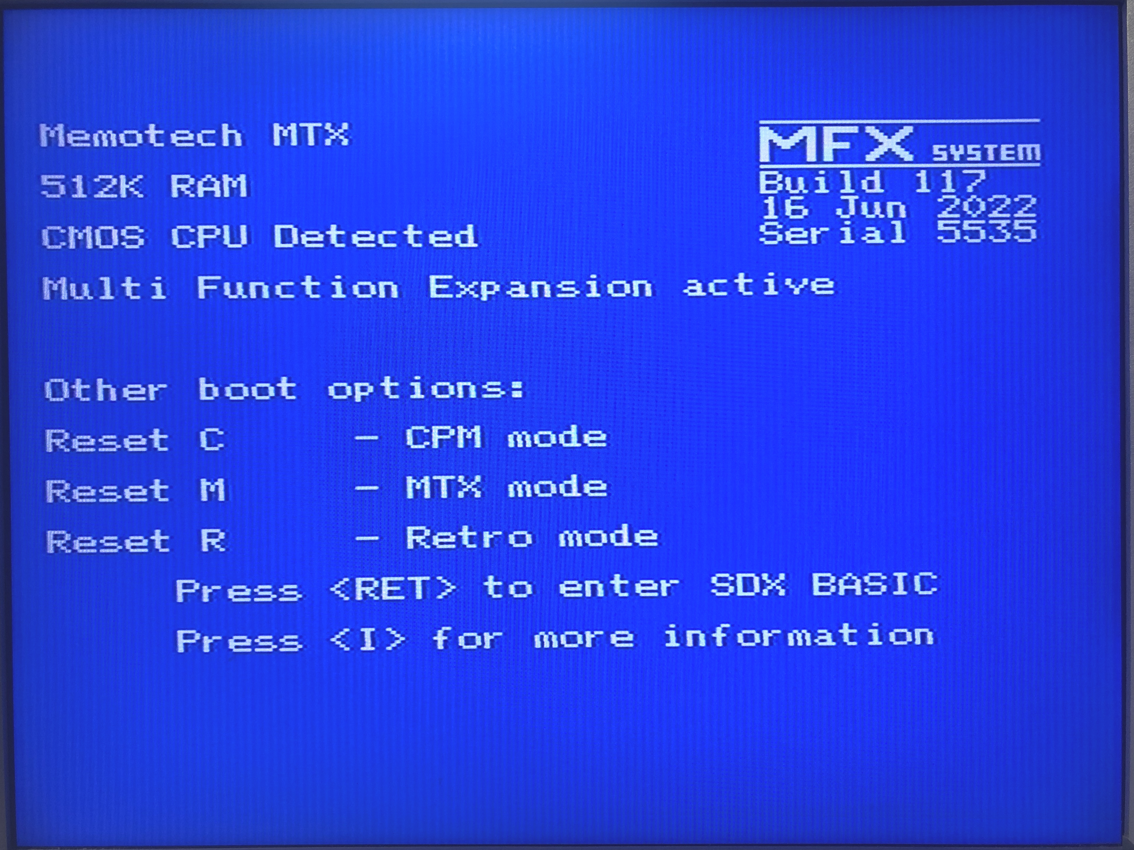
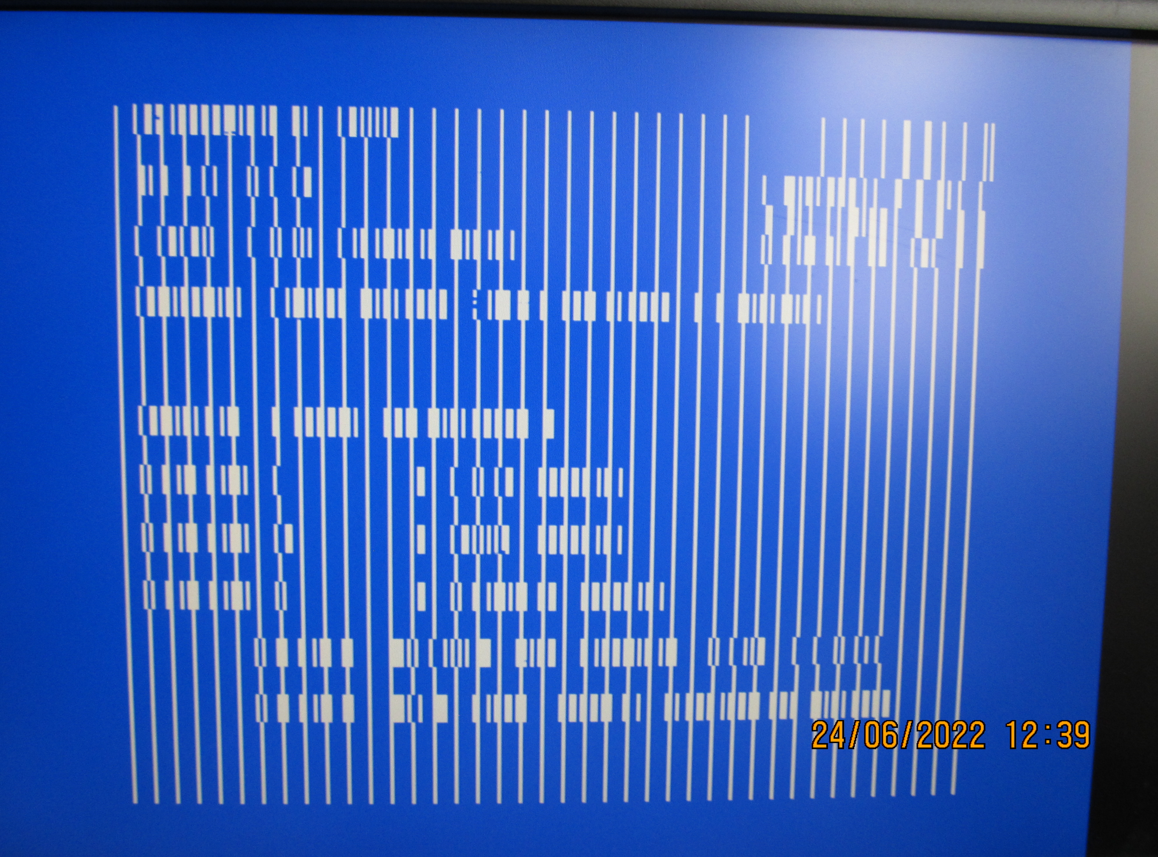
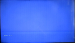
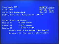
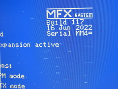
Screen
shot of the MFX boot screen displayed on the VDP output
The system is reporting 512kB of RAM - the maximum
useable. Although 544kB is installed (32k + 512k), this
is constrained by the number of available terms in the
GAL22V10.
The serial number is reporting "noise"
as the ROM cannot read valid data from the FPGA. |
 |
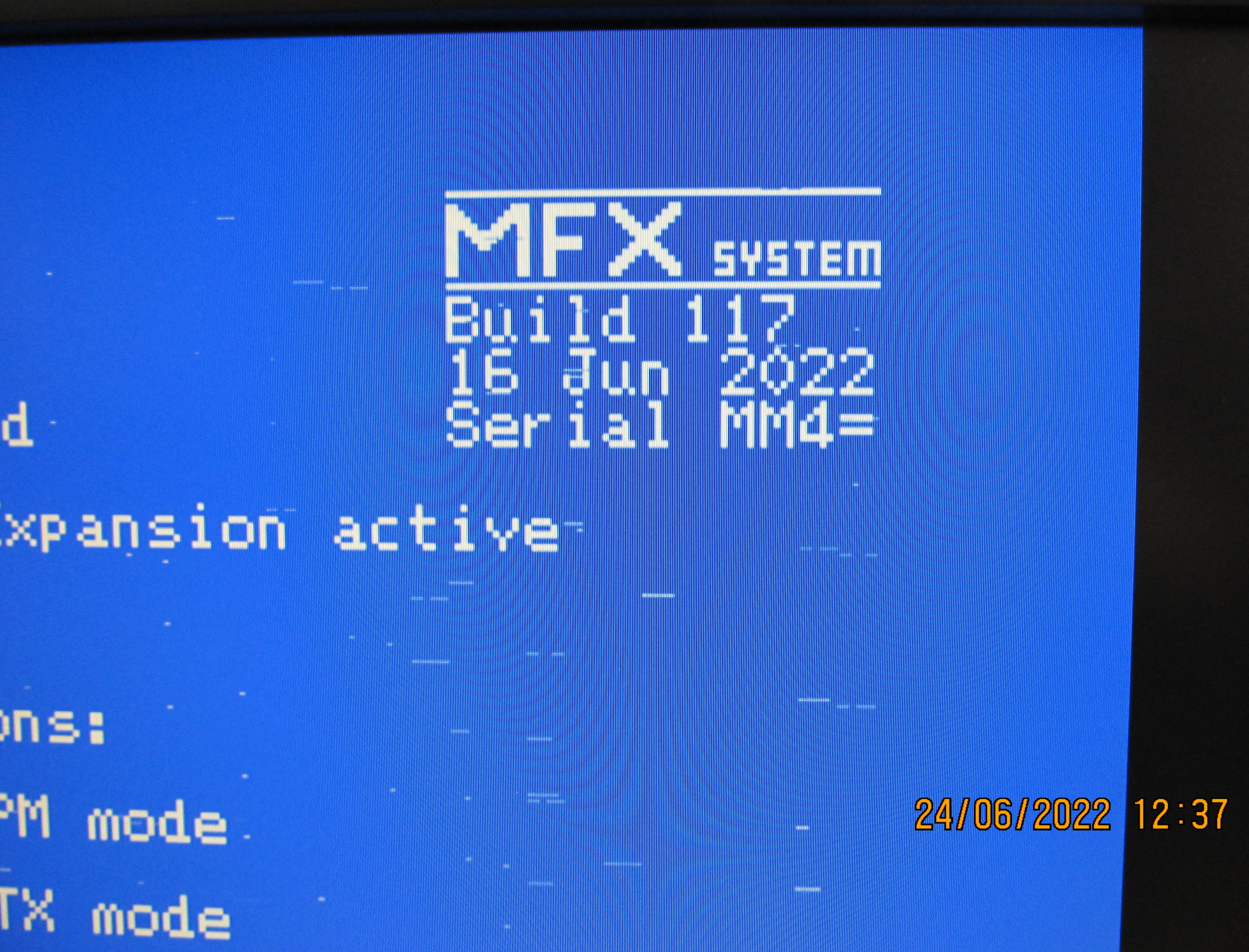
However,
with the FPGA installed, the boot screen displayed on my
VGA monitor was pretty much unreadable. Martin did not
see the same level of corruption on his screen, but he
was using faster VRAM. When when using the same speed as
me (70ns), he got the same results. (Martin also noticed
that I had made a minor error on the VGA pin-out -
another correction to the PCB was needed.)
I
ordered up some faster RAM (Alliance AS6C62256-55) but
my testing was pretty much stalled until it arrived. |
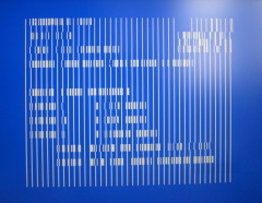 |
With the
faster VRAM, the VGA output from Martin's board was much
better, but did exhibit some noise that was not present
on the prototype board.
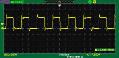
On the boot screen, this
noise appeared as "sparkles", typically looking like a
single pixel line in random character positions as shown
here. These "sparkles" were noticeably worse after an
attempt was made to read the SD card from SDX BASIC. |
 |
The biggest concern
though was that reading the SD card was very unreliable,
more often than not, the system failed to boot to CP/M
and operation of the SD card in SDX BASIC mode failed
too. We lost quite a bit of time here, trying to get to
the bottom of the SD card issue.
During the
development of the prototype
board, Martin had some issues with noisy signals
interfering with the operation of the SD card, but that
was resolved by tidying up the wiring and removing an
unused header. Although there was a little noise on the
PCB SD card signals, it was trivial compared to when the
issue was seen on the prototype.
The most
obvious difference between the prototype and PCB boards
was that the PCB was designed to use one of the common
SD card modules with pull-ups on the data lines. |
| To
eliminate this as a possible cause of the problems,
Martin removed them from his SD card module, but this
did not make a significant difference. |
 |
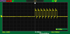
Examples
of the quality of the SD card data signals,
demonstrating that there is no appreciable noise on the
data lines.
(I had made a minor change to the
FPGA I/O allocation to help with routing of the signals
for the PCB, but none of these were associated with the
SD card and in any event, the properties of the relevant
FPGA I/O pins was identical. It turned out that, while
we did consider this as possible cause of the issue, it
proved to be a red herring. |
 |
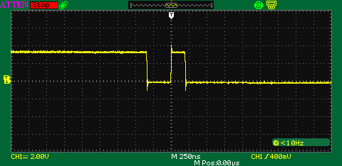
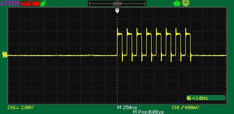
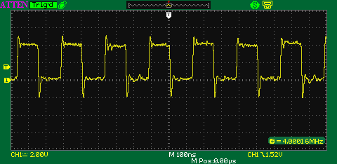
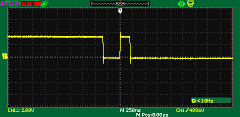
The 'scope
traces show the MTX CPU clock signal on the input and
output sides of the level shifter. The raw clock signal
has a relatively large overshoot on the falling edge but
this is likely not an issue and is much better on the
level shifter output to the FPGA.
Although there
was no indication that there was a problem with the
clock, we discussed the differences between the SD card
implementations in Andy's REMEMOTCH and REMEMOrizer. In
REMEMOTECH, the whole MTX is synthesized in the FPGA and
the SD card is clocked by the FPGA at 25MHz. In
REMEMOrizer, the SD card is clocked by the MTX CPU at
4MHz. |

 |
The SD interface in
MFX was changed to mimic that it REMEMOrizer, i.e., it
was clocked at 4MHz and the data transfer synched to the
MTX clock. This resolved the SD card issues.
This was particularly puzzling as the
SD card worked without issue on the prototype, the
interface between the FPGA was simple and the PCB
checked out fine. However, since the switch to the
REMEMOrizer like implementation resolved the issue,
there was no real need to investigate further.
The video noise ("sparkles") was equally puzzling - the
video on Martin's prototype board was perfect but
building the hardware on the PCB had made things worse!
We spent a lot of time checking that the PCB was
consistent with the schematics and Martin's blocking
diagram. Martin also spent a lot of time checking for
noise and other issues but was unable to spot anything
untoward.
The eventual "fix" turned out to be
quite interesting too.
The FPGA allows the user
to configure a range of drive strengths for the I/O
pins. The range for LVTTL (3.3v) is from 4mA to 24mA
with the default at the higher level. Tucked away in the
device data sheet is the text "Using minimum settings
provides signal slew rate control to reduce system noise
and signal overshoot ". When Martin changed the output
pin configuration from 24mA to 4mA, the "noise" issue
magically went away.
Again, the fact the
prototype board did not have the "sparkles" problem was
interesting, but as the issue now appeared to be
resolved, no further time was spent on it - following
the guidance in the data sheet seemed to do the trick! |
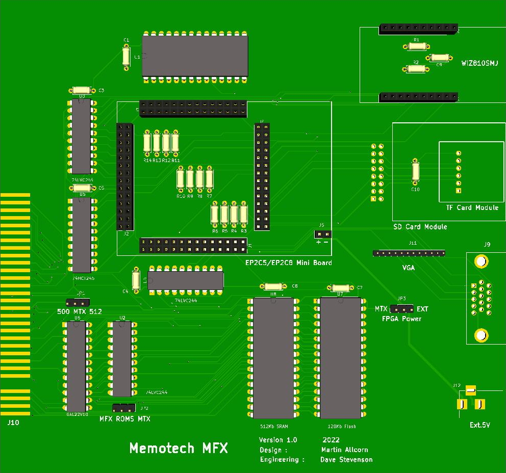
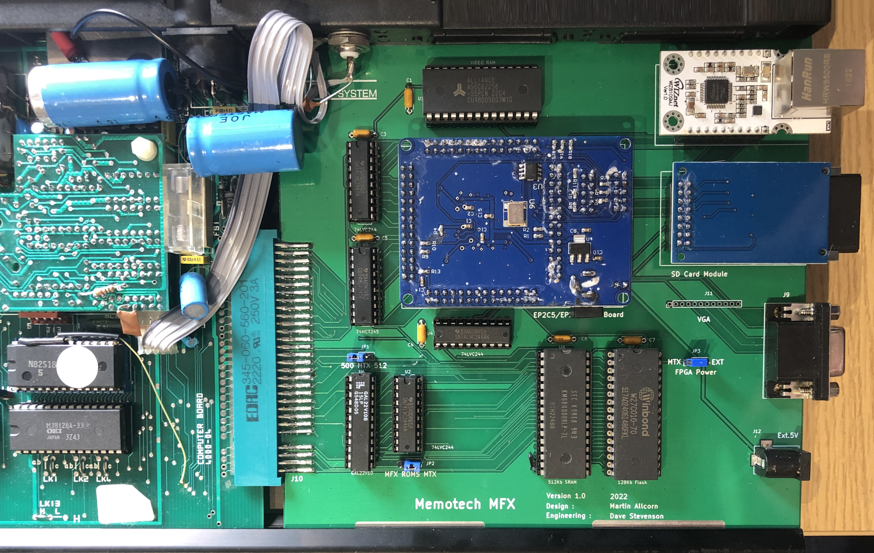
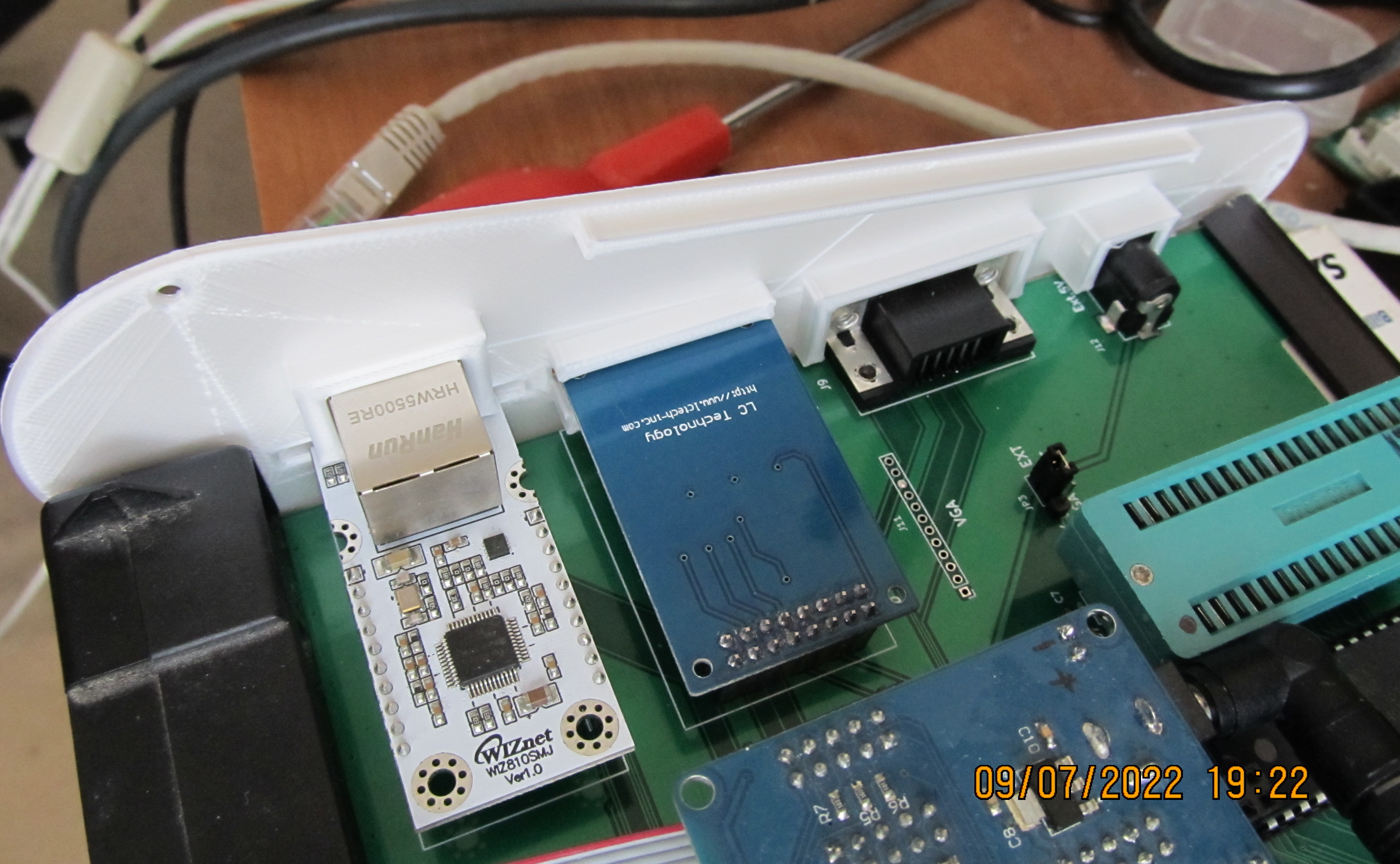
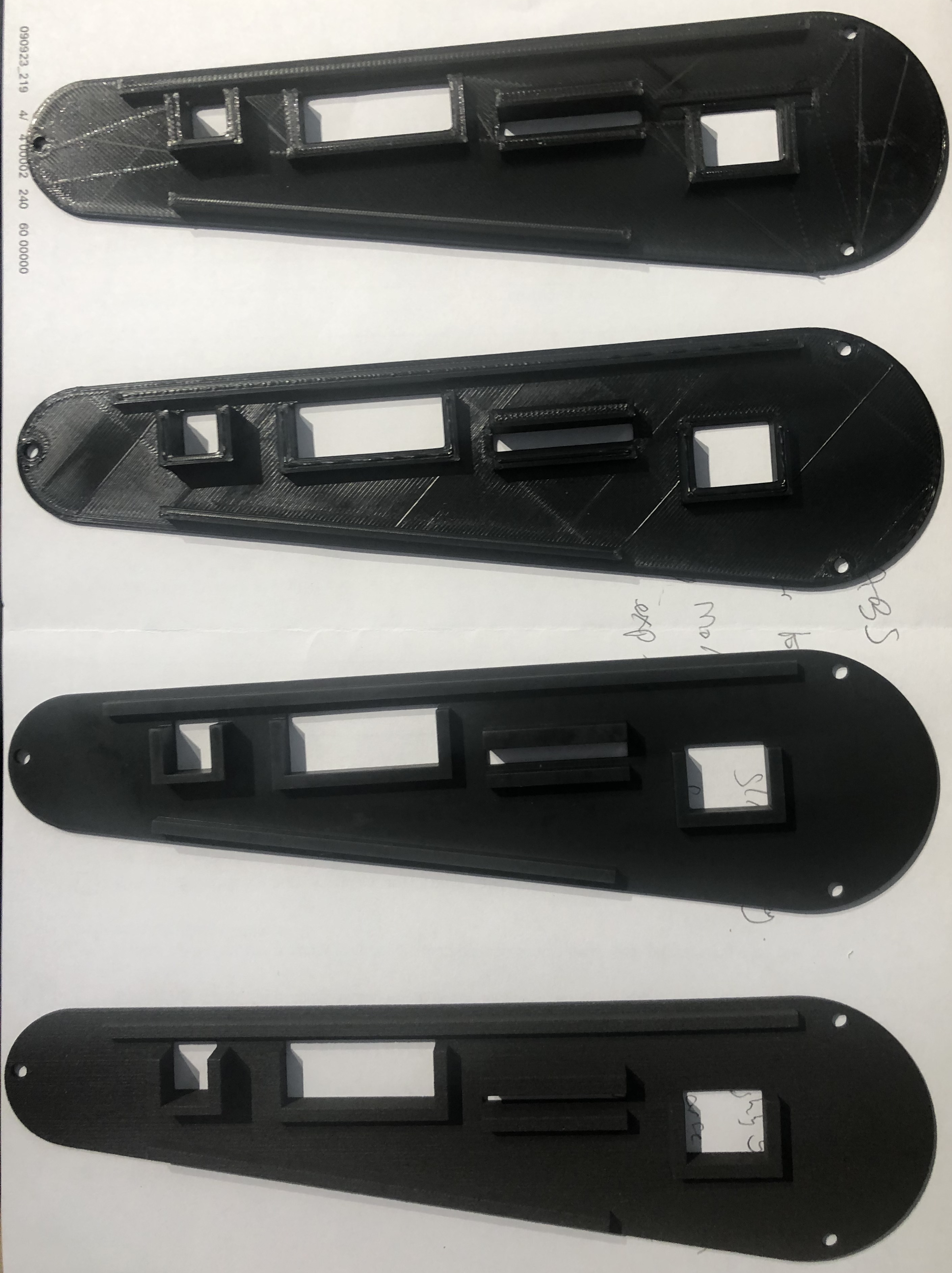
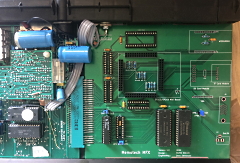
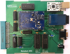
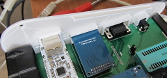
The fully
assembled PCB, with all its sub-modules fitted
The large blue board is the FPGA module
The smaller board is the SD card module
The white module is the WIZnet network adapter
(The FPGA module arrived with a few areas of excess
solder flux, it looks a bit ugly, but as it does not
affect its operation, didn't bother to try and clean it
off.) |
 |
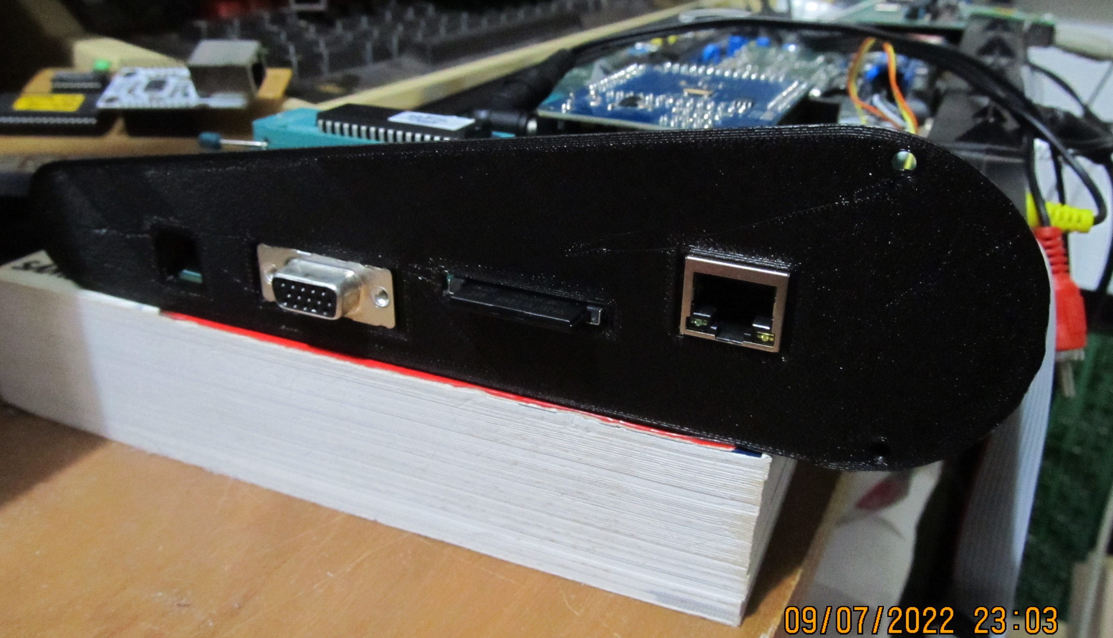
| Installed
in the MTX |
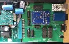 |
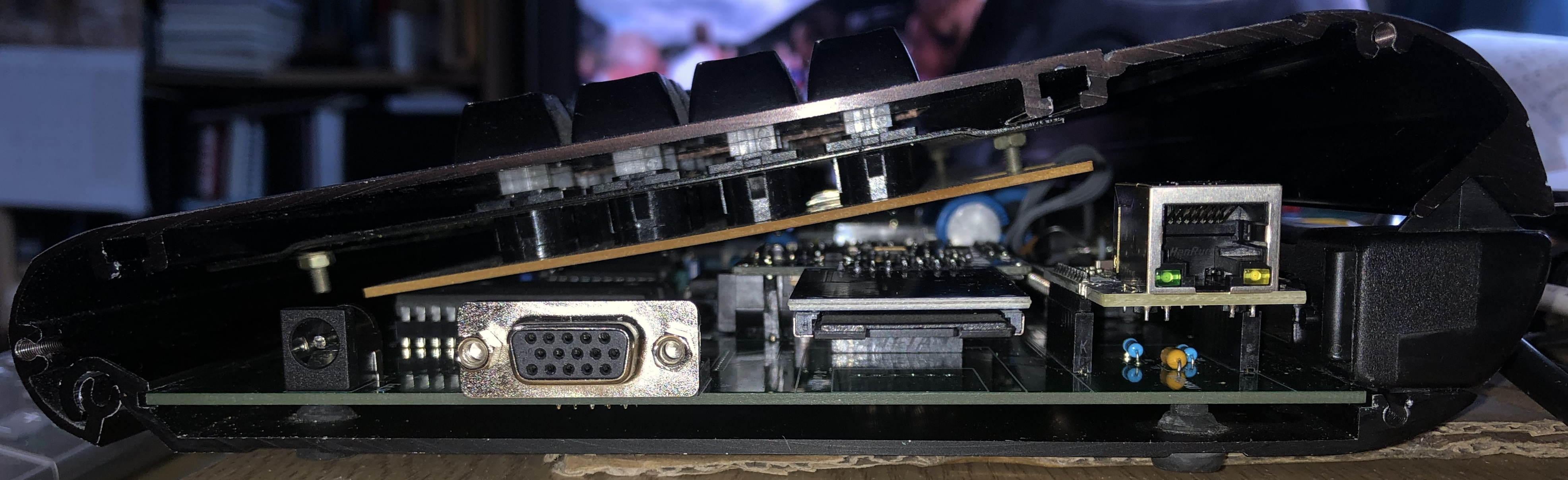
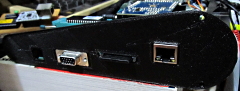
| End on
view, showing the fit of the FPGA, WIZnet and SD card
modules below the MTX keyboard PCB. As anticipated, it's
neat, but it fits with no problems. |
 |
Just as we thought
that we were done, a really worrying issue came to
light.
Although the WIZnet interface seemed to
be working fine, we found that intermittently, files
transferred to the MTX over using FTP had errors when
they were saved to the SD card. One rare occasions, the
odd byte was being dropped from the file. For example,
when sending over an 8kB RUN file, one byte towards the
end of the file had been missed and the subsequent data
was shuffled up in the file. Strangely, when copying the
same file multiple times, most were OK, but perhaps 1 in
10 was missing the same byte in the saved file.
Quite a bit of time was lost trying to locate the source
of the issue; the signals to the WIZnet module appeared
to be "clean" and "noise" didn't really explain how the
same byte could be missed on just the odd occasion.
The WIZnet module used the CPU's Read (\RD) and
Write (\WR) signals. These signals are driven by the CPU
at one end of the MTX computer board and are distributed
to various locations on the computer board and around
the MFX PCB. Thinking about the positive effect that de-glitching
the CPU clock signal had had, Martin wondered whether
de-glitching the Read and Write signals for the WIZnet
module might improve things.
Fortunately, there
were two spare I/O pins on the FPGA module that could be
used for this purpose.
Martin modified his PCB
and added logic to de-glitch the signals for the WIZnet
module.
Ta-Da! After testing multiple transfers,
Martin was confident that this had resolved the issue.
We don't quite understand why this is the case, but
Martin theorized that it may be due to the way the the
WIZnet auto increments the pointers after a transfer
like the VDP does. However the WIZnet is MUCH newer so a
glitch that goes un-noticed by the older devices gets
accepted as an valid transaction, when the proper signal
arrives it too starts a transaction, but the pointer has
moved.
In any event, the important thing is that
the issue has been resolved. |
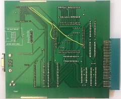
The modification on my PCB
It
was a fairly simple task to break the traces for the CPU
Read and Write signals below the WIZnet module and patch
the pins to the spare I/O pins on the underside of the
FPGA module. In true Memotech fashion, I used yellow for
the patch wires :-)
As with Martin's PCB,
extended testing demonstrated that the issue had be
resolved. |
 |
| By now,
Martin had also produced a design for the 3D printed end
plate. Here you can see his test print using white
filament. |
 |
As well as
being cheaper than the black filament that will be used
for the final print - the white allows the detail to be
seen more clearly.
You can see how Martin has
added small shrouds around the connectors to increase
the rigidity of the thin end plate. |
 |
| Whilst the
positions of the connectors were acceptable, they were
not exactly flush with the printed end plate. Moving
them a couple of mm here and there will allow them all
to be flush and look better. |
 |
So, it's done - Almost !
The two PCBs assembled by Martin and myself, with
the minor modifications described on this page, are
working as designed.
Having proven the design, I
had planned on using the additional PCBs that I have
left over from the first production run to supply "early
adopters", but the need for the two patch wires has made
me reconsider that. Whilst they are on the underside of
the PCB and will never be seen once the PCB has been
installed, I don't like them - though they do look like
a lot of Memotech's boards :-)
My intention now
is to get another run of PCBs done to incorporate the
changes to the WIZnet configuration, in addition, I will
take the opportunity to correct the other minor issues
identified with the V1 board :-
Correction to the solder mask layer
Correction to the VGA connector pin-out
Reduce board width by 1mm to increase clearance to the
end plate
Minor I/O connector
placement changes to better align with the end plate
|
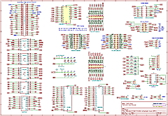
Final
version of the schematic
- incorporating the
WIZnet modifications
Version 1.1 of the PCB has
been ordered to this design. |
 |
OK,
updated PCBs have arrived and they appear to be OK.
I have just ordered some trial pieces of the 3D
printed end plate (in different materials) and have just
started assembling the first few "production" MFXs. They
will be ready to ship once I have checked the fit of the
end plate - probably another 10 days. |
 |
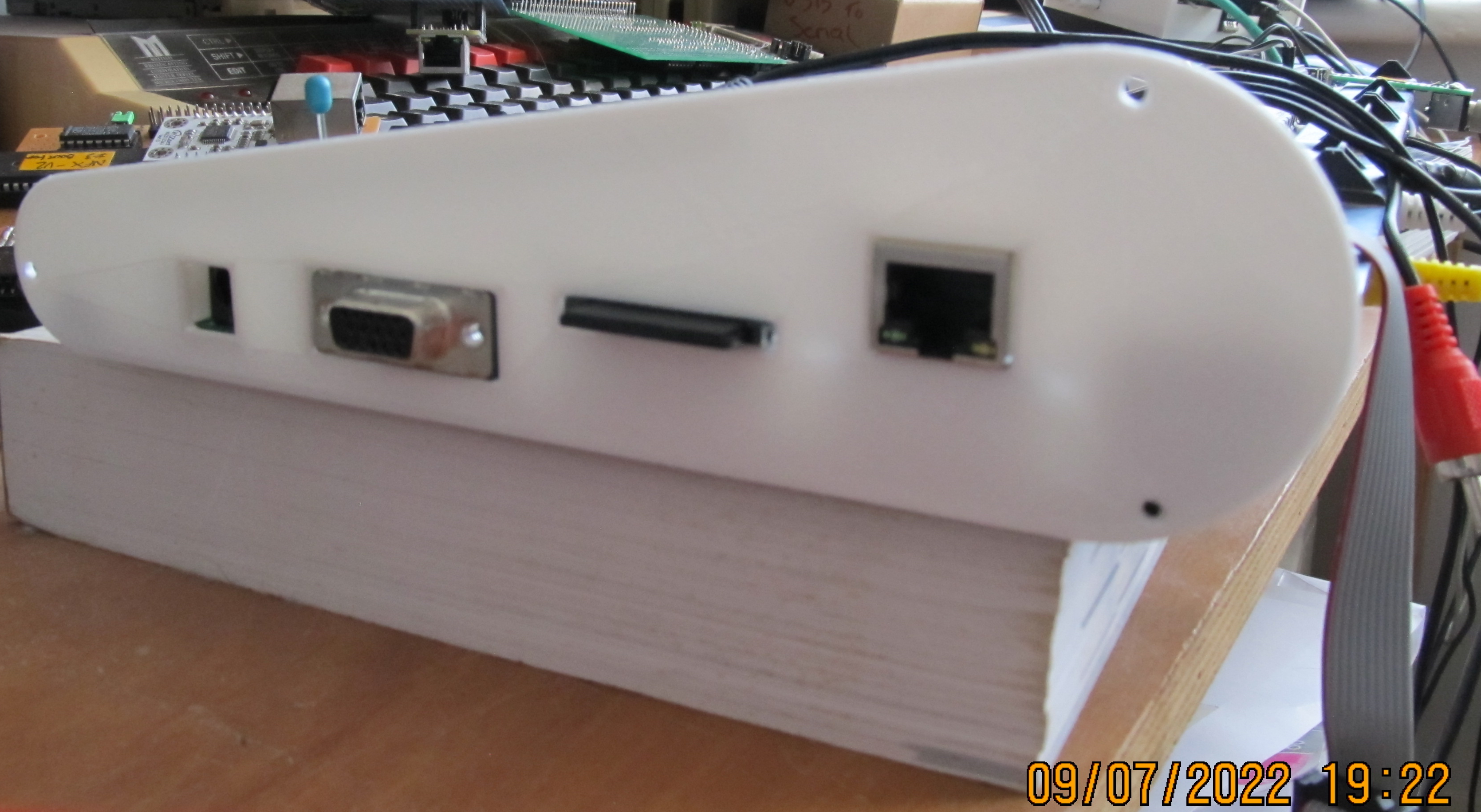
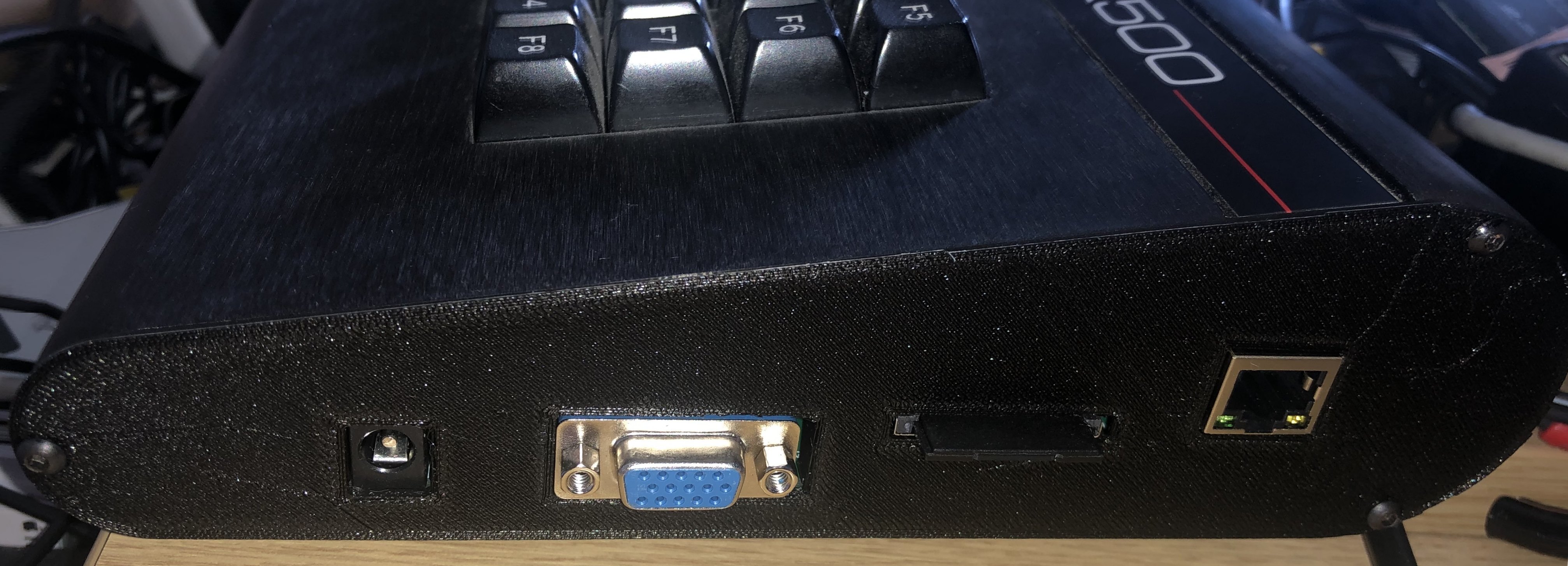
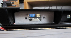
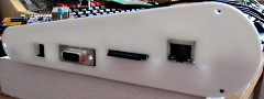
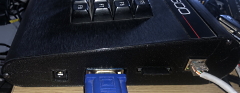
| Martin
sent me an end plate that he printed on his 3D printer,
shown here fitted to my MTX500 with VGA and network
cables attached and the SD card inserted. It has a
slightly textured finish, but other than that, it
completes MFX perfectly! |
 |
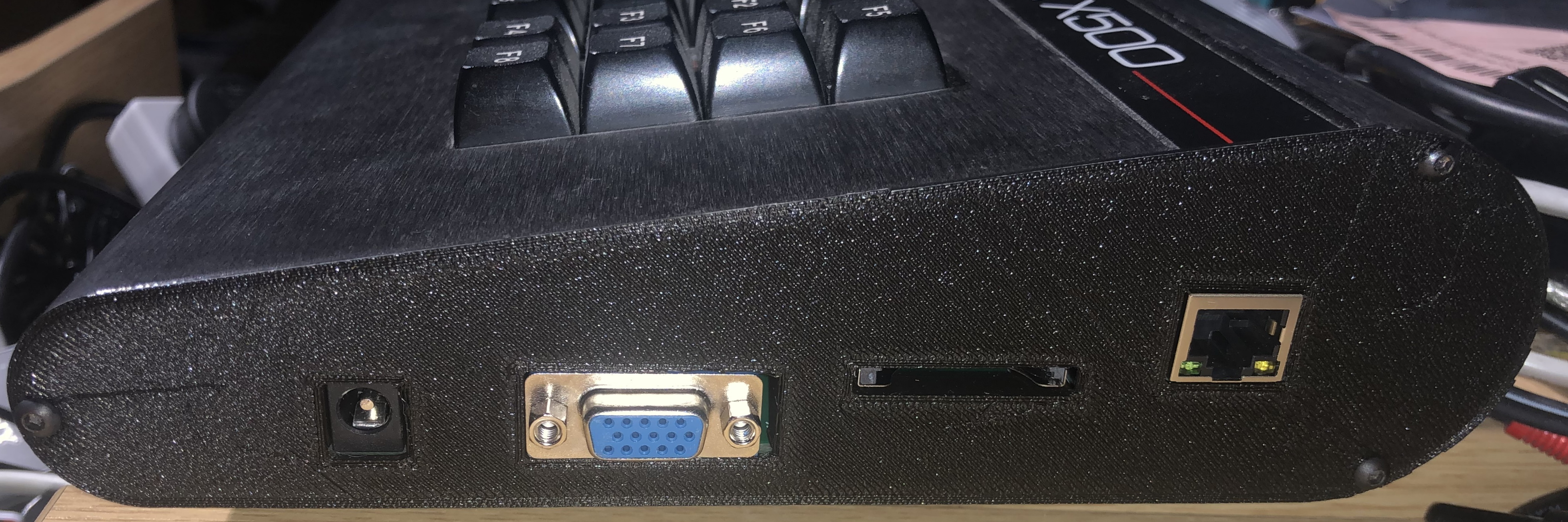
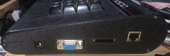
| And here
with the cables disconnected. |
 |
| And the SD
card removed. |
 |
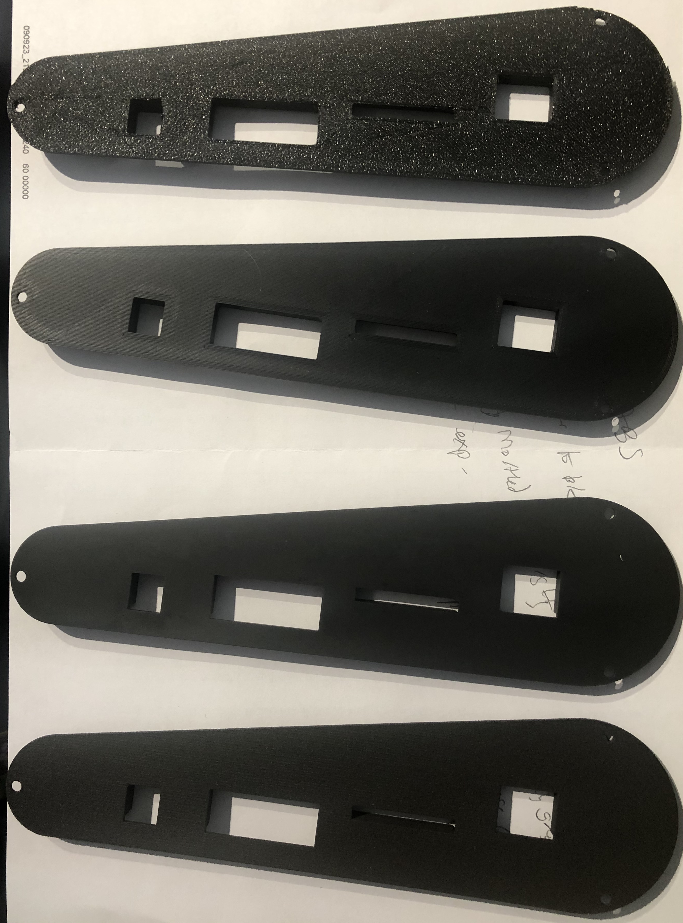
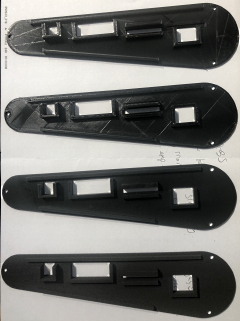
The 3D end
plates that I ordered from a commercial 3D printer have
now arrived, apologies for the poor quality photos, but
hopefully, you can see the differences between them -
particularly if you open the full size photos.
From top to bottom . . .
Martin's example
FDM(ABS)
SLA(Resin)
SLS Nylon
The
three bought in items all have pretty good print
quality, the difference is obviously in the materials
used. My observations are : |
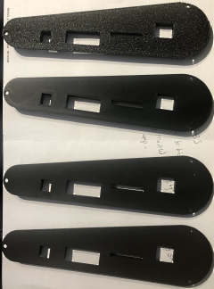 |
FDM(ABS)
The most expensive
The "blackest" of the three Slightly grainy finish
Perhaps the most rigid
SLA(Resin)
The cheapest, 40% of the ABS price
Mid range colour between the ABS and SLS
Very smooth finish, pretty close to the texture of the
Memotech
metal end plate
Not quite as
rigid as the ABS, but there’s not much in it
SLS
Nylon
The mid range material,
half way between the cost of the others
Quite coarse texture
Probably the
least black one, slightly grey looking
A little more flexible than the others, but still
acceptable |
 |
Although the
colour is slightly greyer than I'd have liked, if I do
go to this vendor, then I think that the cheapest
material is actually the best. The smooth texture looks
the best of all three, but based on the samples above,
other than convenience, there is probably little to
choose between a "home" print and a professional one.
In terms of colour, Martins filament gives a
much "blacker" finish than the commercial version,
though the surface finish is not as nice; this is a
function of the print bed that Martin uses, other 3D
printers have a glass print bed which will likely
produce a much smoother finish - closer to that of the
commercial resin print.
|
| |
|