The following pages contain references to my
KiCad schematic of the 80 Column board,
signal names defined on the schematic are indicated like this (SRLD)
and the locations of the ICs on the 80C PCB like this (A1).
Display Generation
The 80C card incorporates a "high speed"
15MHz "dot clock"
which is used to generate the timing and
control signals for the shift register,
latch and video output circuits external to
the CRTC. The Motorola
MC8645P datasheet gives the maximum
clock frequency of the CRTC as 3.0MHz, for
the 80C card, the dot clock is divided by a
74LS161
synchronous binary counter (in board
position F7) to produce
the CRTC clock signal (CRTCLK) of 15/8,
i.e., 1.875 MHz which controls all timing internal
to the CRTC.
The data to be written to the screen is
stored in the refresh memory by the CPU,
normally as an
ASCII code which cannot be
directly
displayed as a character. On the 80 Column
card, the standard set of 128 ASCII codes is
supplemented by the additional codes
required to produce the extended character
sets. The character
generator ROMs are used to convert the ASCII
code into the dot pattern that makes up the
character presented on the screen, for the
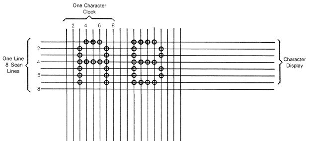
80 column card, each character is made up
from an 8 x 8 matrix of pixels (including
the blank pixels required to allow space
between the characters & rows).
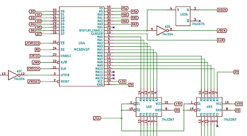
The CRTC
generates memory addresses (MA0 to MA13)
used to scan the refresh RAM (MA11 to
MA13 are not used in the 80C board), row addresses (RA0 to RA4)
used to address the character generator ROM
(RA4 is not used in the 80C board) and the video timing signals, vertical sync
(VS),
horizontal sync (HS)
and display enable (DE). Since the refresh
RAM must be accessed by both the CPU and the
CRTC, access to it must be multiplexed using
logic external to the CRTC.
Operation of the 2K SRAMs is controlled by
the Chip Select (CS),
Output Enable (OE)
and Write Enable (WE)
signals, on the 80 column card,
CS is tied to 0V, meaning
that the chips are always selected, memory
read is enabled by
OE (6116OE) and memory write is
enabled by the
WE signals (ASCWE
and
ATRWE ). The ROMs
contain the dot patterns required to
reproduce the character in the screen as an
8 x 8 matrix.
When the CRTC is required to display the
character in a given screen position, the
ASCII code for the character at that screen
position is used to locate the required bit
pattern for that character in the
appropriate ROM. The CRTC uses the row
address bits to locate the line in the ROM
character that corresponds to the scan line
position of the character being displayed.
Each time the screen is redrawn, starting
with the first character position on the
display, the CRTC reads the ASCII code in
the corresponding memory location in the
refresh RAM and puts the value of the
character on the "private" CRTC data bus,
the CRTC also puts the appropriate character
row address on the row address lines.
The
ASCII code and row address are used to get
the required bit pattern to display on the
scan line from the
character or graphics ROM, for the 80 column
card, the 8 bits are loaded into a 74LS166
(A6)
parallel-in, serial-out shift register
(using the Shift Register Load
signal, (SRLD)
from where
the bits are output sequentially under
control of the Shift Register Clock
(SRCK) clock to generate the
monochrome video data signal (VCNTL).
The attributes of the displayed pixel are
updated from the Attribute byte controlled
by the Attribute Clock signal (ATRCK)
(at the same frequency as
CRTCCK.
Under the control of the
VCNTL
signal, the 74LS157 (E7)
quadruple 2-line to 1-line data selector
switches between the foreground (VCNTL
= 1) and background (VCNTL
= 0) attribute to set the appropriate video
signals ON or OFF.
Under the control of the Video Clock signal
(VCLK),
the 74LS175 (E5)
quadruple "D" type flip-flop latches the
state of the video outputs until the rising
edge of the next
VCLK signal.