|
 |
The Memotech MTX Series |
 |
PAL14L4 Reader for the
Memotech MTX
Given that there are 14 inputs, there are "only"
16384 (2^14) possible input combinations to drive the four
possible outputs. Tony Brewer made a PAL14L4 Reader
and wrote the Z80 code to control it. It takes just
over 10 seconds @ 4MHz to step through all of the
possible input combinations and read the 16K nibbles
of output, search for active low outputs, remove
redundancy and give the logic expressions as a text
string, e.g. XX X010 000X 1111
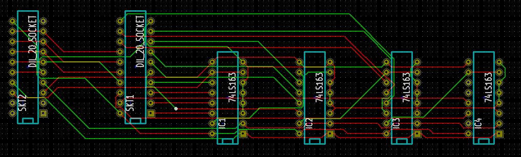
With Tony's help, I have drawn up a schematic for
the PAL reader interfaced to the MTX User I/O Port
using
KiCAD.
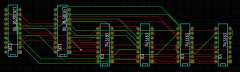
| Despite a few limitations, KiCAD allows you to take
a design all the way from a schematic through to the finished
PCB.
Using the KiCAD design suite, including the
on-line automatic "router", can produce finished
designs such as this board for the PAL Reader. |
 |
However, it is uneconomic to have a board professionally made
just for a single unit, so an alternative solution for
the production of a working prototype was called for.
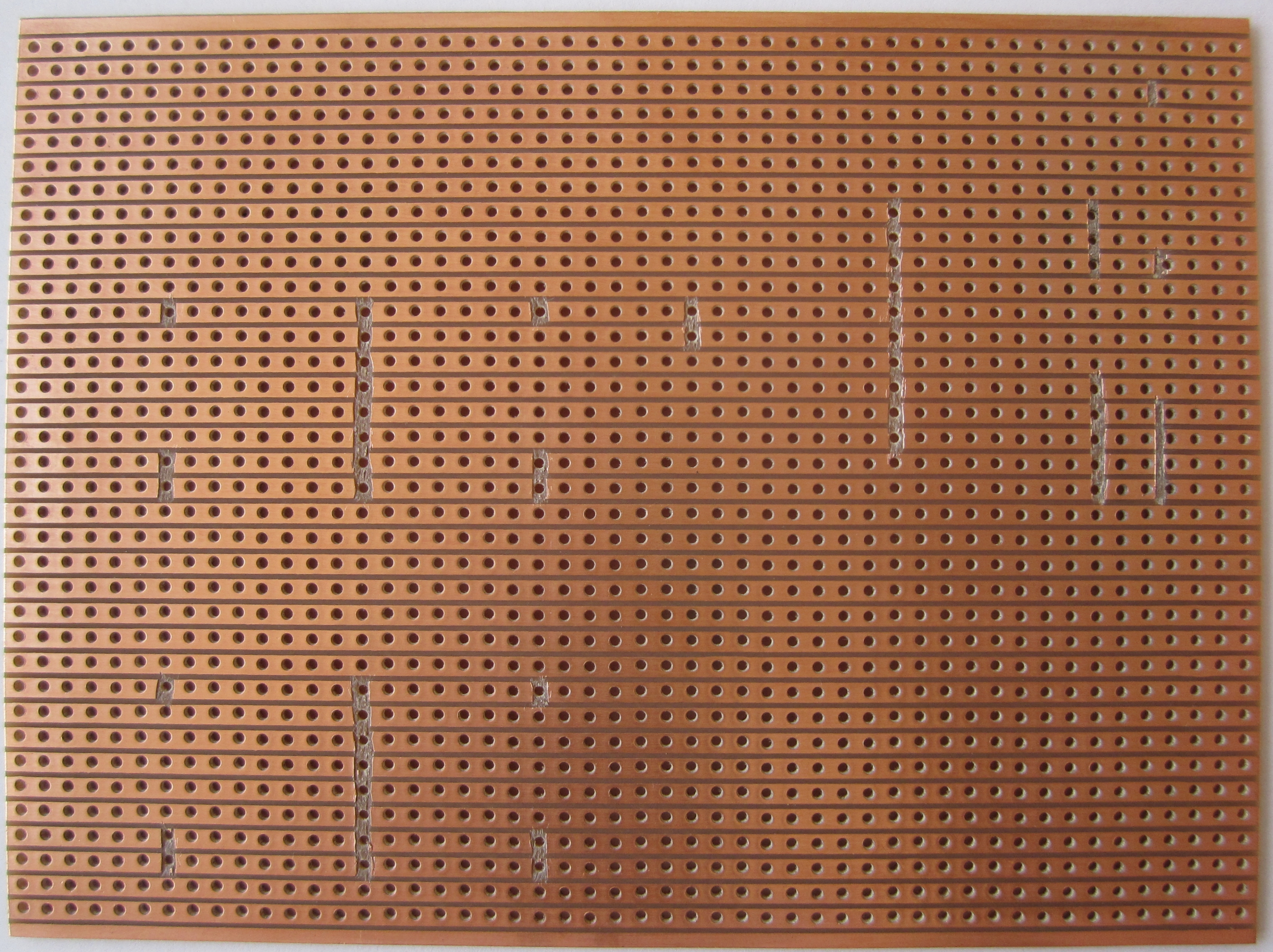
Stripboard
is a widely used type of prototyping board, and ideally, I would
have liked to have used a stripboard add-in for KiCAD.
Unfortunately, I could not find a free add-in that would have
done auto-routing of a KiCAD schematic, so I had to use a
stand-alone stripboard design program. I looked at a number of
free stripboard design tools including Stripboard Magic
(would not run on Windows 7), Stripboard Designer 1.0
(extremely basic), VeeCAD
Free (black and white only) and
VeroDes (written in VB5). Whilst it did look good, I was
originally put off by VeroDes by its requirement
to install a host of dependencies before the program would
install on Windows 7 and was intending to use VeeCAD Free,
being a bit reluctant to have VeroDes screw up my
Windows 7 machine. However, Tony had successfully used
VerDes and recommended it, so I installed it after all.
While I was having a go at designing the layout and routing
myself, Tony quickly came up with a VeroDes
design, which I have to say, is far batter than the attempt that
I would have made. Simple things (being easy when you know how)
like tying unused inputs and outputs together on chips having
these signals on opposite sides by not cutting the stripboard
between them saves cluttering the board with unnecessary links.
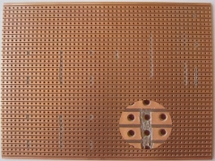
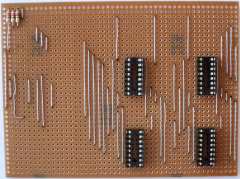
Having seen a photo of Tony's prototype board, I had bought
some stripboard (95 x127 mm) that I thought would have been more
than adequately sized, as it turned out, if it had not been for
Tony's compact design, I would have struggled to fit the parts
on my board without it becoming an untidy mess.
|
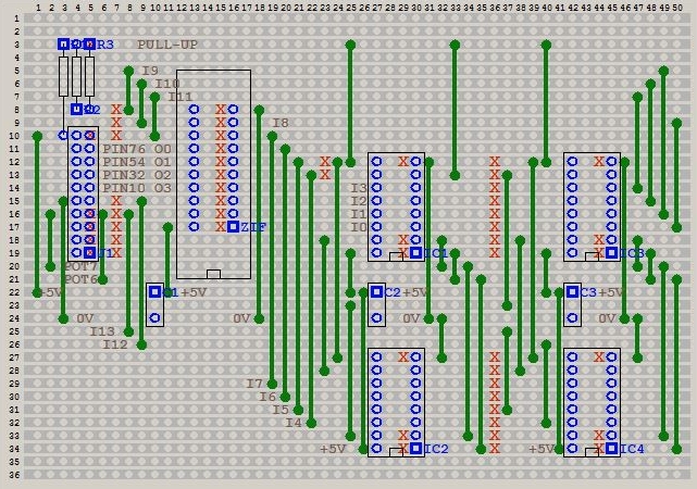
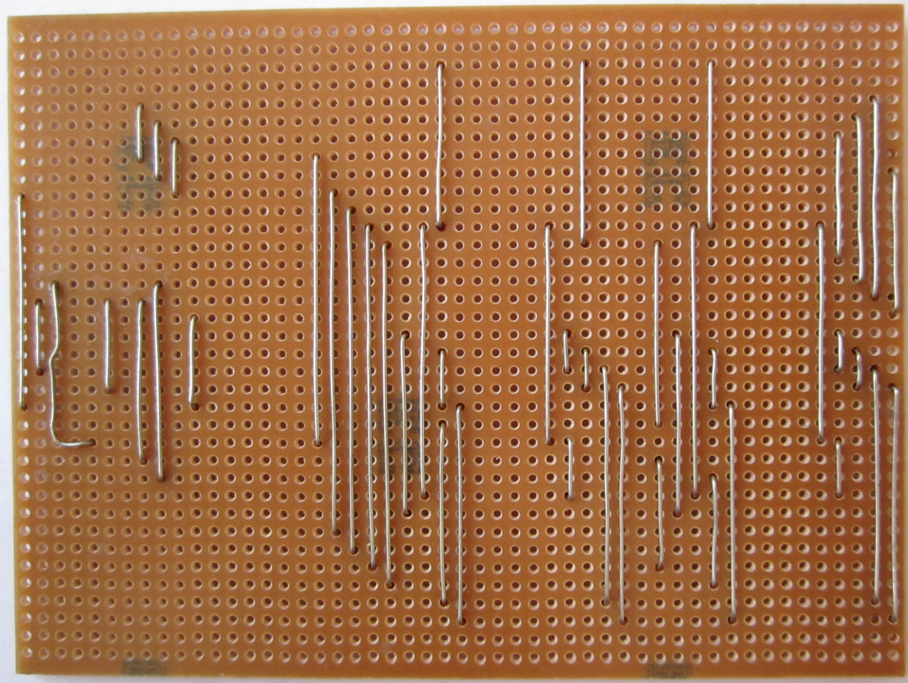
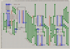
Tony's VeroDes design for the PAL
Reader. The green lines indicate the wire links on the
component side of the board and the red "X"s
denote breaks in the tracks on the solder side.
Normally, these are at holes, but for the IDC
connector, the break must be between the connector
pins and respective holes. VeroDes
is not able to show this accurately and breaks must
be shown aligned with the holes. (This prototype
uses the 5V supply from the MTX I/O port -
see below for why this
is not feasible and for the finished design.) |
 |
|
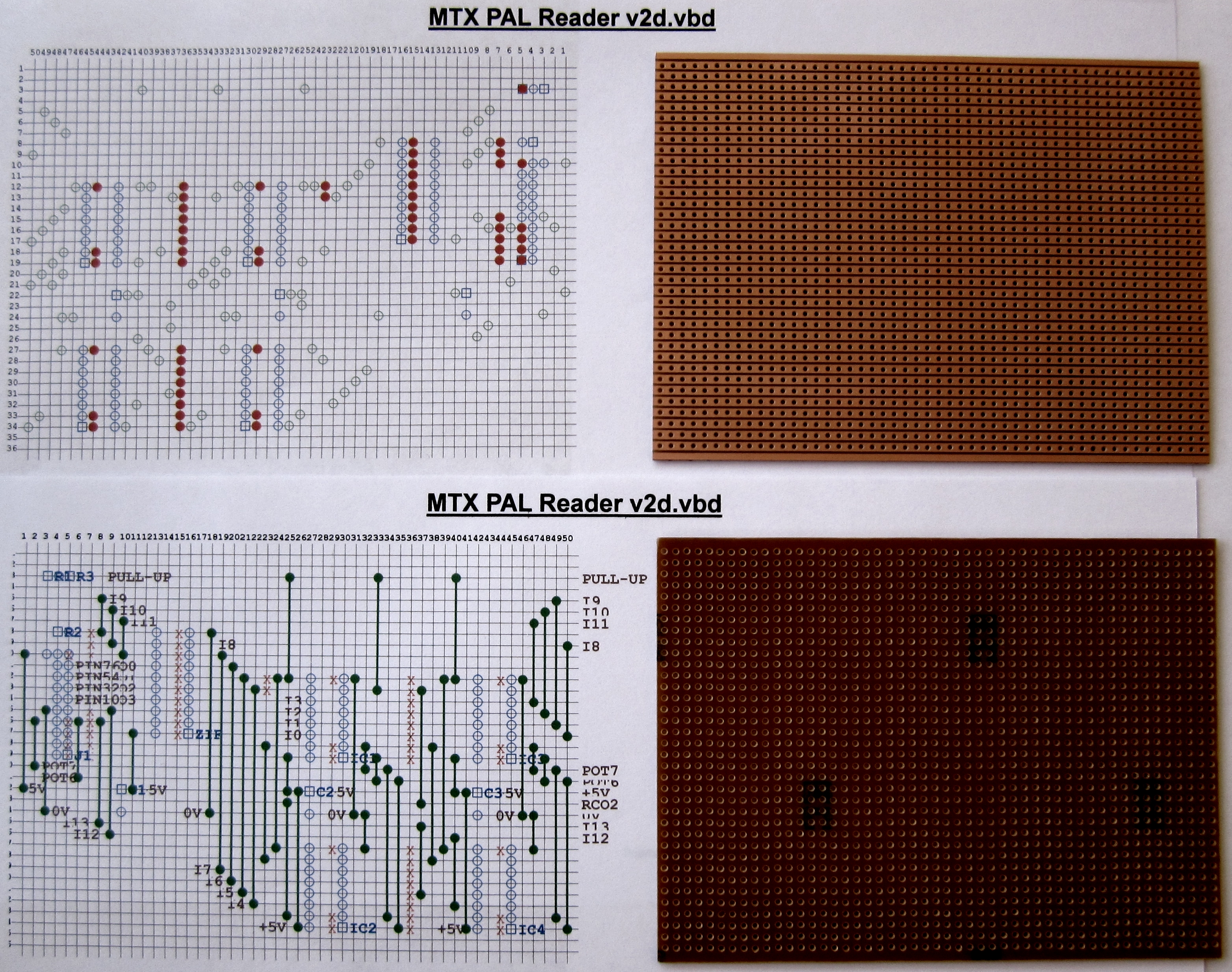
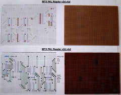
A really useful feature of VeroDes is
its ability to print overlays for the copper and
component sides of the strip-board, these can be
used to place the components and identify the track
breaks and wire links required. On the solder side
overlay, the position of the track breaks are
indicated by the red dots and the link ends or
component legs, by the grey circles. |
 |
|
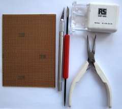
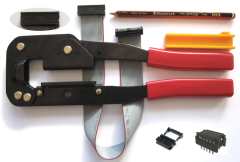
Preparing for the "operation", scalpel at the ready! -
The surgical mask and gown are just out of shot :-)
[If I do something like this again, I will
invest in one of those hands free solder stations
with a light and magnifying glass - it would have
been a great help - particularly when cutting the
tracks and checking the solder joints at the end.] |
 |
|
The first task was to make the required cuts in the
tracks. You can buy track cutters for stripboard,
most of these are basically just a drill bit in a handle
that is turned on a hole to cut the narrow strips of
copper on either side of the hole.
(These tools are not suitable for cutting the
strips between holes.) |
 |
|
When making the track breaks it's wise to "measure
twice, cut once" !
I had intended to use the trimming knife just to
make the cuts that were positioned between the holes
and to use a drill bit to cut the rest. Using the
knife, two parallel cuts were made through the
copper layer and the copper picked off with the tip
of the knife.
Since the knife was working well, I used it to
make all of the cuts. Once all the cuts had been
made, I smoothed off the cut edges of the tracks and
used a multi-meter to make sure that there was no
continuity between the two sides of the cuts. |
 |
|
When cutting the tracks, I obviously handled the
board a fair amount which, more than likely, had
transferred some "grime" onto the copper tracks.
Prior to soldering, I used a PCB eraser (a small
rubber block with a fine abrasive embedded) to clean up
the strips and gave the board a final wipe over with
isopropyl alcohol to ensure a clean surface for the
solder to adhere to. |
 |
|
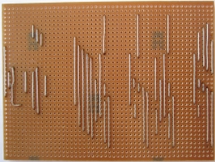
The first
"components" to be mounted were the wire links.
As well as identifying the positions of the
links by their x,y coordinates, the
VeroDes component overlay was very
useful for making up the links themselves.
Starting at the right hand side of the board, I
first made a 90o bend on one end of a
piece of link wire and laid the link on a copy of
the overlay to measure the required length, prior to
making the second 90o bend. The links
then had bends at the correct distances to
match the holes in the stripboard and could just be
dropped into place prior to soldering and cutting
off any excess length with a pair of small side
cutters. |
 |
|
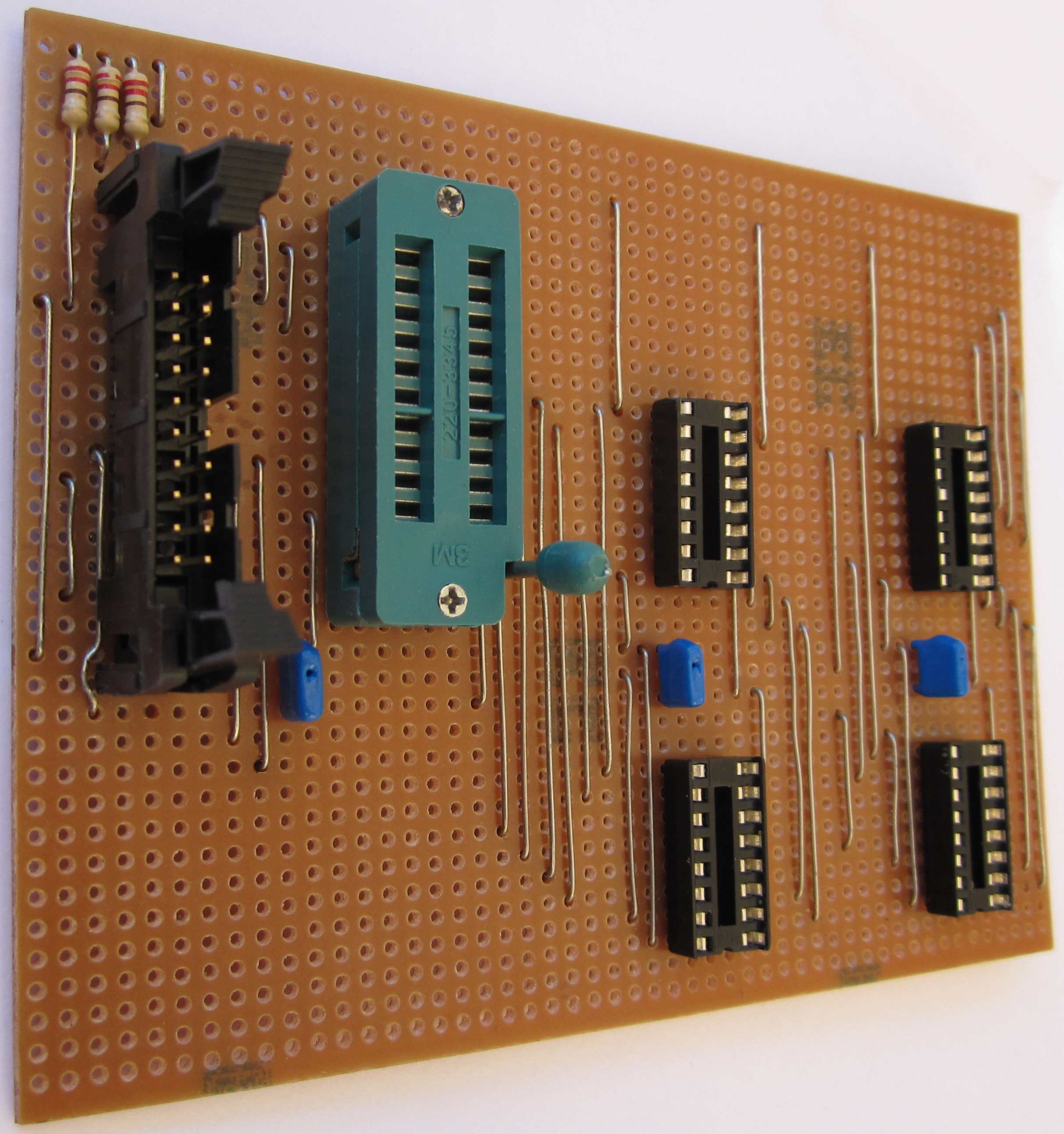
The resistors were installed next, followed by the
sockets for the counters. An observant reader may
have noticed that the resistor positions do not
match the schematic. The design was based on a plain
IDC header, as I had bought one with latches, to
allow for the extra length of the connector, the
resistors had to be relocated further up the board
and an additional cut was needed in the track
between the bottom of R2/R3 and the I9 input.
Similarly, the link from the header to the 0V
line had to be modified to clear the bottom of the
longer IDC connector, resulting in the "L" shaped
link. |
 |
|
After the IDC header was installed, I found that it
was possible to get the 0V link to clear the bottom
of the connector by making a small radius curve at
the bottom end. This meant that the unsightly "L"
shaped link could be replaced with a vertical link
to match the others. The ZIF (Zero Insertion
Force) socket for the PAL has also been mounted at
this point, you can see that the locking lever is in
the open position. ZIF sockets should be soldered
with the contacts in the open position to reduce the
risk of soldering the contacts together when
installing it.
Self adhesive silicon rubber feet were then
attached to the solder side of the board to provide
a stable base and ensure the solder joints were
clear of the work surface. |
 |
|
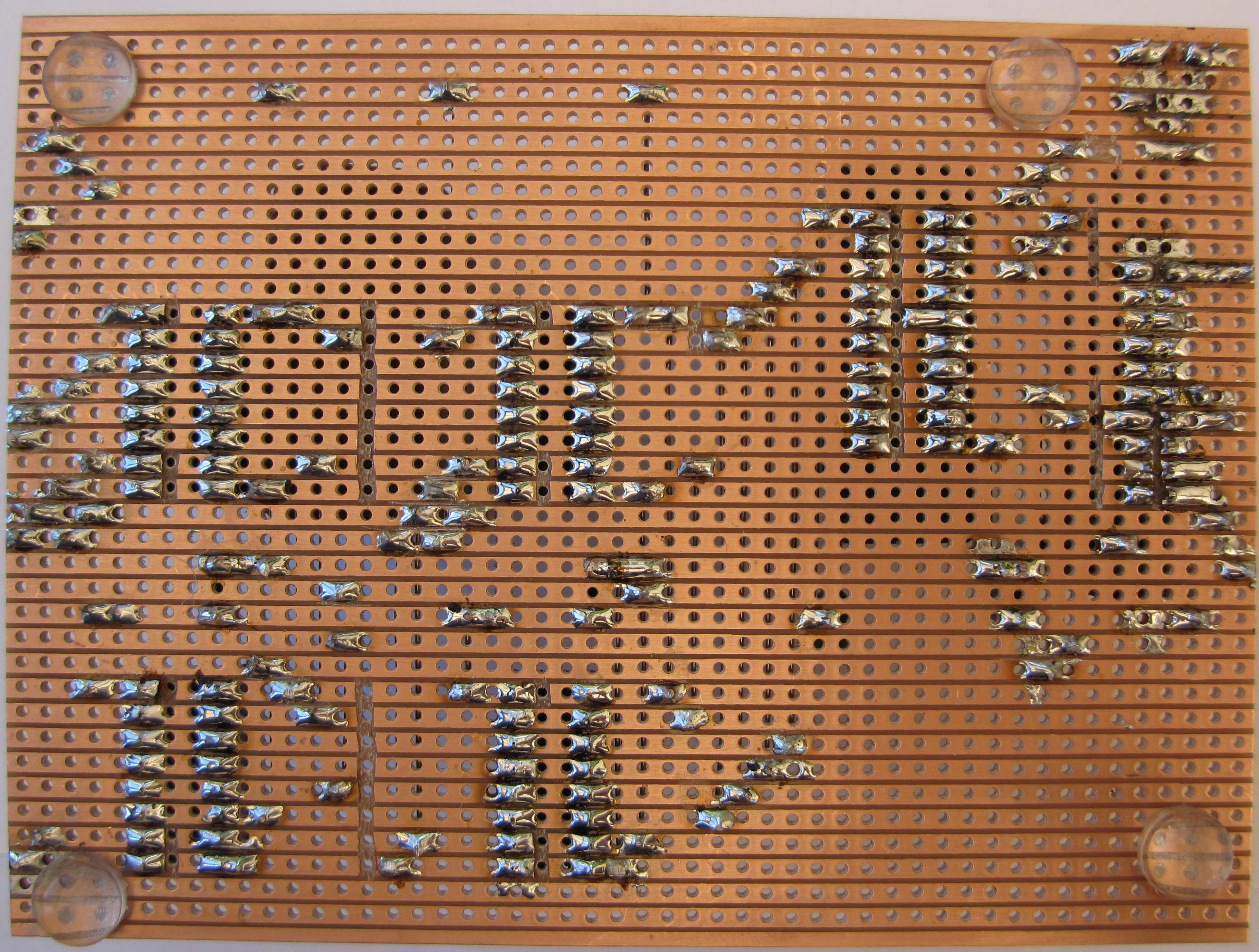
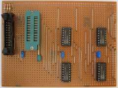
Solder side of the completed board, exposing my
(lack of) soldering skills! Prior to installing
the counters, the tracks were visually checked with
a magnifying glass to ensure that no solder joints
had overflowed onto adjacent tracks or across track
breaks and that any solder "splashes" had been
removed.
The board was also checked with a multi-meter to
ensure that there was continuity and no short
circuits between the lines shown on the schematic,
with particular attention being paid to ensuring
that there were no shorts between 0V and 5V. |
 |
|
The board is wired to the MTX I/O port with 20 way
ribbon cable with an IDC plug on one end and a 20
pin DIP plug on the other. The cable should be as
short as possible, although I needed it to be ~12"
long to sit on top of my FDX just behind the MTX.
With the proper tool, crimping of the IDC plug is
quite easy, the DIP plug is a little more awkward,
but I found that a hexagonal pencil was just the
right size to fit between the legs to protect them
while crimping the plug. |
 |
|
|
|
Installation & Testing |
|
|
|
|
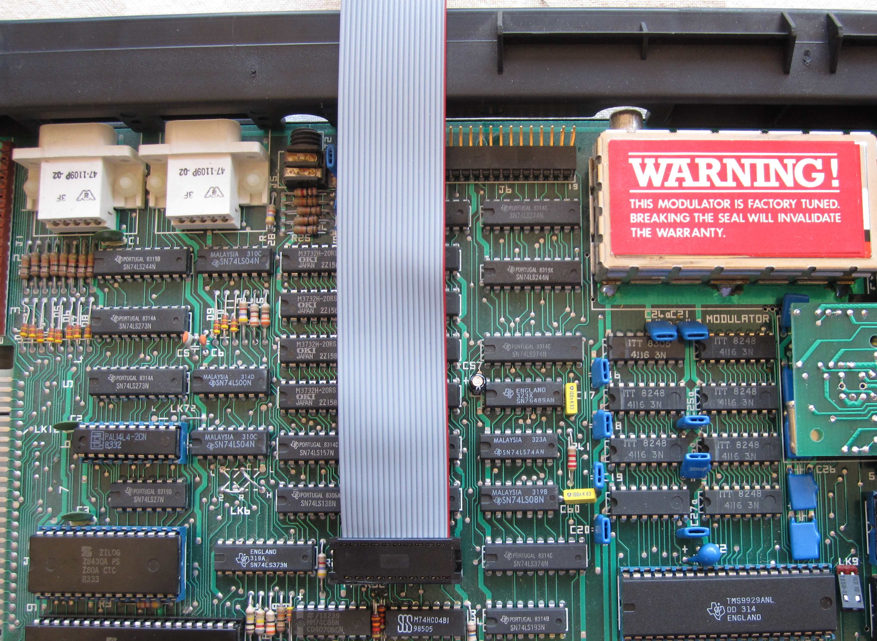
The User Port interface is the blue 20 pin DIP
socket located at position 8C on the main board.
When installing the DIP header into the I/O socket,
pin 1 of the cable, identified with the red-stripe,
must be installed in pin 1 of the DIP socket. NB:
The User Port socket is installed the opposite way
around to all of the ICs on the board - pin 1 is the
connection on the upper right hand side of the
socket - on the ICs, it is at the lower left. |
 |
|
The ribbon cable connected to the I/O port and
exiting the case above the printer interface
connector. I found that the DIP plug did not make
a very secure connection to the I/O socket and taped
the ribbon cable to the flat on the cut-out above
the printer port. |
 |
|
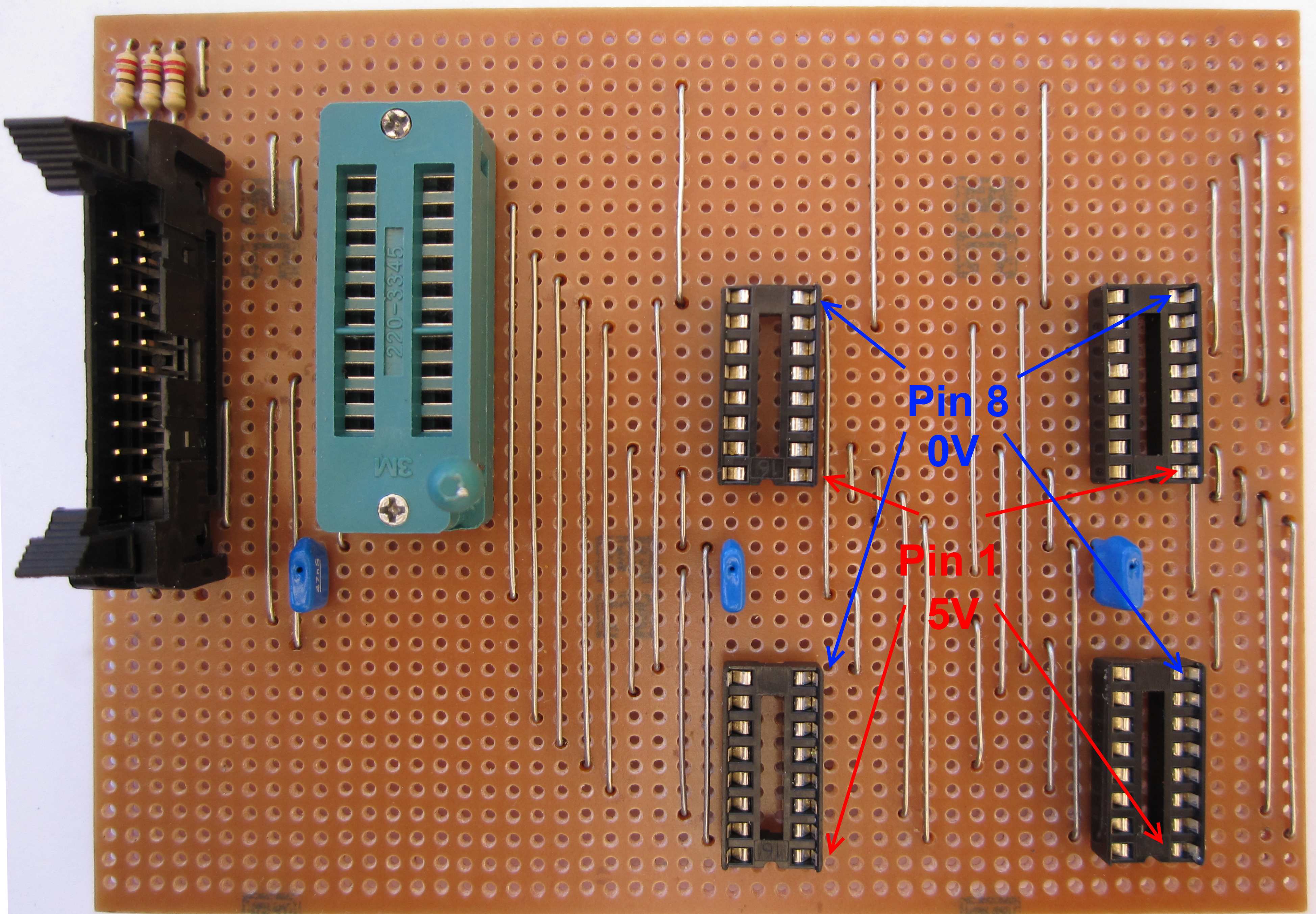
The board was initially connected to the MTX
(with the power OFF) with all of the sockets empty.
When the MTX was powered ON, a check was made to
ensure that 0V and 5V were
present on pins 8 and 16 of the 74LS163s and pins
10 and 20 of the ZIF socket. The 5V supply from the
MTX connected to pin 11 of the IDC header was also
checked. |
 |
|
To verify
that the counters can be correctly controlled from
the MTX, the following code can be used and the
voltages on the
CLR
and CLK pins measured on any of the counters. The
expected voltages on the pins are shown in the
table.
XOR A
OUT 7,A
;POT7=0, POT6=0 [From BASIC,
OUT 7, 0]
LD A,40
OUT 7,A
;POT7=0, POT6=1 [From BASIC,
OUT 7, 64]
LD A,80
OUT 7,A
;POT7=1, POT6=0 [From BASIC,
OUT 7, 128]
LD A,C0
OUT 7,A
;POT7=1, POT6=1 [From BASIC,
OUT 7, 192] |
|
74LS163 Voltages |
| Pin 1 (CLR) |
Pin 2
(CLK) |
| |
|
| 0 |
0 |
| |
|
| 0 |
5 |
| |
|
| 5 |
0 |
| |
|
| 5 |
5 |
|
|
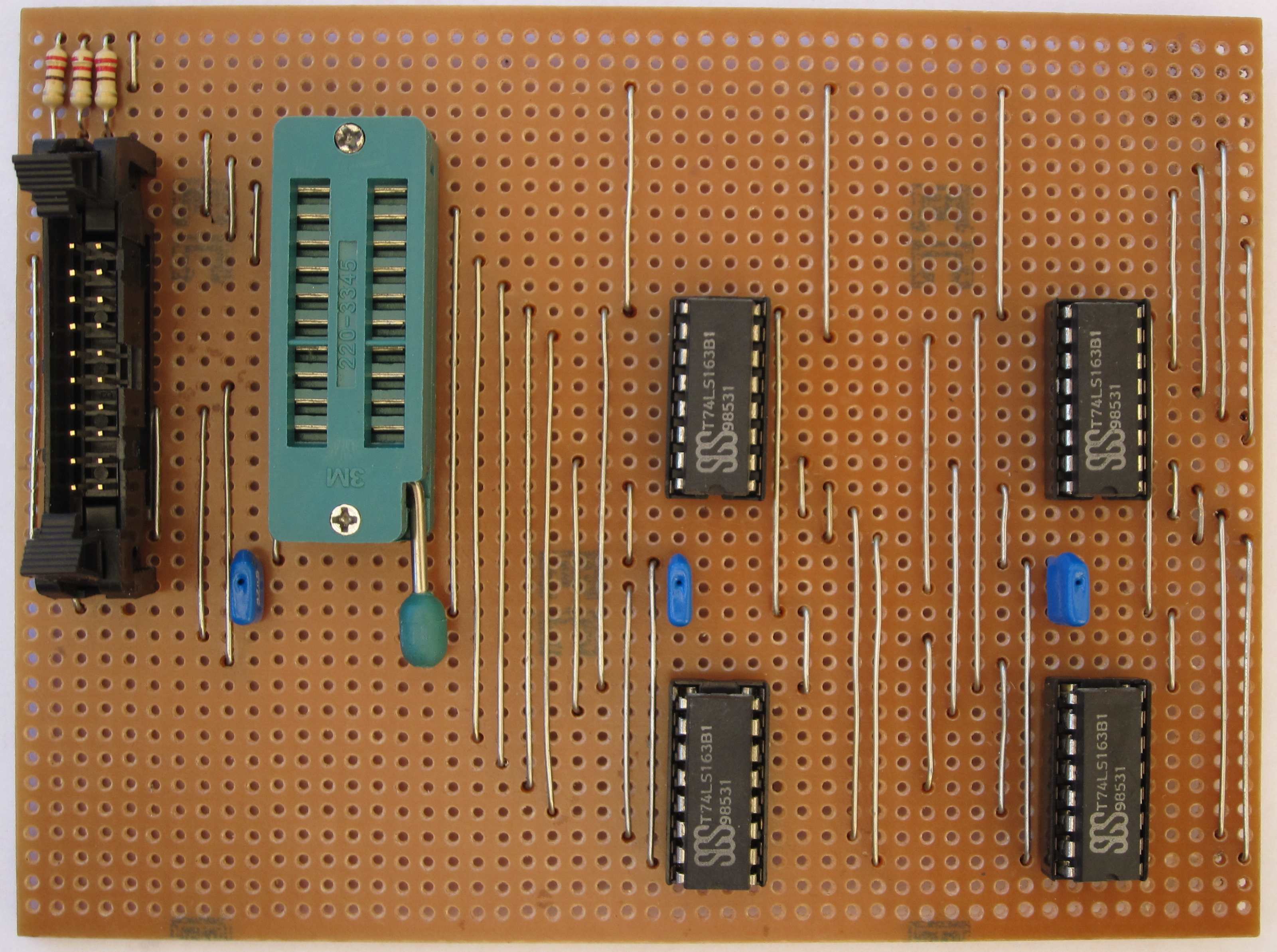
After verifying the
supply and counter control voltages, the MTX was
switched OFF and the counters were installed in the
sockets.
When the
MTX was switched back ON and the voltages rechecked
I ran into a problem, the supply
voltage had been pulled down to less than 1V.
According to the MTX manual, the
MTX is only capable of supplying a maximum
of 20mA from Port 7 and the counter datasheet states
the typical power dissipation is 93mW, i.e., 18.6mA
per counter. With 4 counters on the board, I thought
that the Port 7 5V supply was not going to be adequate for the
counters. |
 |
|
An
external 5V supply was required, fortunately, I had
enough bits & pieces to hand to make a suitable
modification.
A two pin
header was added to allow connection of an external
5V supply and the 5V line from the MTX was
disconnected by breaking the track at position 3,10.
A new link was installed between 12,22 and 12,23
with an additional break at position 15,23.
The
modified VeroDes design is as shown. |
 |
|
With the
external supply connected, the following code was
used to check that the counters
were incrementing as expected
XOR A
OUT 7, A
LD A, 80
OUT 7, A
LD C, 40
LD B, 0
LOOP: LD
A, 40
OUT 7, A
LD A, C0
OUT 7, A
DJNZ LOOP
DEC C
JR
NZ, LOOP |
|
Zero "A" |
|
Reset all POT bits (clears counters) |
|
POT7 |
|
CLR = 1, i.e., NOT clear |
| |
| |
| |
| |
| |
| |
| |
|
Counter incremented |
|
Repeat . . . . |
|
until . . . . |
|
All 16384 counts done |
|
|
|
|
|
If all of the tests are
successful, the PAL Reader is now ready for use
Return to the
main PAL Reader page for
info on using the tool |
|