|
Z80 Special Reset
Although not mentioned in Zilog
databooks the Z80 CPU supports two
types of reset cycle, normal and
special. A normal reset disables the
maskable interrupt, selects
interrupt mode 0, zeroes registers I
& R and zeroes the program counter
(PC). A special reset only does the
last of these. Zilog literature also
states that
RESET must be active for at
least three clock cycles (3T) before
being properly accepted. Tests with
short reset pulses 1T or 2T long
have shown that this is not true and
the reason for Zilog saying
otherwise is explained later.
What is the special reset?
US Patent 4486827 describes the
Z80 special reset and the abstract
is succinct:
"A special reset function is
provided in the CPU, using the same
control input to the CPU as a normal
reset, to reset only the program
counter to facilitate the use of a
single CPU in a microprocessor
development system."
The patent document should be
downloaded to learn more about the
intended application of the special
reset. It enables breakpoints whilst
debugging Z80 code that preserve the
complete state of the system, except
for PC which is easily saved.
Nothing is put on the stack unlike
when taking a "snapshot" using the
non-maskable interrupt (possibly
destroying data) and in any case the
NMI pin might not be
available. Sharing the same 64K
address space does mean that during
development the user cannot access
the very top of memory where the
monitoring software is located but
changes to assembly code to cater
for this are normally trivial.
I used such a development
system, a Zilog in-circuit emulator
(ICE), whilst working for Memotech
at Oxford and Witney thirty years
ago but was unaware of the special
reset and the crucial part it played
in the ICE until a few weeks ago.
How the special reset is
generated
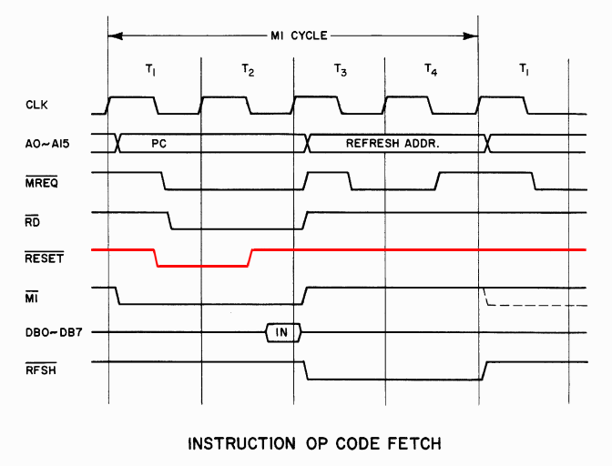
Very precise timing is required
to generate a special reset signal.
The figure above shows a Z80
instruction opcode fetch (M1 cycle).
To be special
RESET must be low only at the
rising edge of clock state M1T2 as
shown in red (the low pulse width is
illustrative). A reset will be
normal if
RESET is low at any rising
edge of CLK other than M1T2. The
results of tests with reset pulses
1T and 2T long during M1 cycles are
shown below. (Other M cycles were
not considered as a special reset
during these is impossible.)
RESET low at rising edge
of Type of
M1T1 M1T2 M1T3 M1T4 .... reset
X Normal
X Special
X Normal
X Normal
X X Normal
X X Normal
X X Normal
X X Normal
Note that a reset pulse that is very
short (much less than 1T long) will
still generate a reset provided the
minimum
RESET to rising edge of CLK
setup and hold times are met. For
the Z80A these are 60 ns and 0 ns
respectively for the NMOS version or
60 ns and 10 ns respectively for the
CMOS version. (The 10 ns hold time
for CMOS also applies to
WAIT,
BUSREQ and
INT.)
How the CPU detects the
special reset
Below is a modified version of
Fig. 11 from the patent with changes
made for clarity and consistency.
The external logic with two D-type
flip-flops is just one way to create
the special reset pulse (note that
M1 here is
M1 inverted). In the tests
performed the
RESET signal was a registered
output from a programmable logic
device (PLD) clocked on the falling
edge of CLK, enabled when
M1 is low and
MREQ is high for the special
reset.
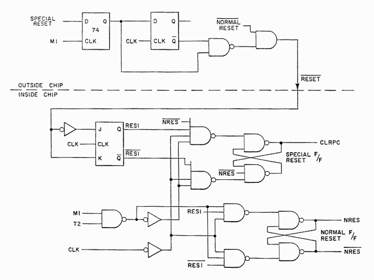
As there is only one reset pin
the Z80 designers needed to include
extra circuitry to distinguish
between the two reset functions.
Inside the chip are the equivalent
of three D-type flip-flops, two with
enable and one with enable and
clear. The RESI f-f samples the
RESET input on every rising
edge of CLK, the normal reset f-f
samples RESI on every falling edge
of CLK except in M1T2 and the
special reset f-f samples RESI on
the falling edge in M1T2 only.
NRES acts as an asynchronous
clear for the special reset f-f.
After
RESET goes low during M1T1
RESI goes high on the rising edge of
M1T2 and CLRPC goes high on the
falling edge. If
RESET is still low at the
next rising edge (at the start of
M1T3)
NRES will go low on the
falling edge and clear CLRPC.
Similarly if
RESET is low at the rising
edges of both M1T1 and M1T2
NRES will prevent CLRPC going
high.
Therefore a 2T reset pulse is
sufficient to produce a normal reset
provided the minimum setup and hold
times are met and the tests shown
earlier prove this to be the case.
However an asynchronous reset signal
cannot be relied upon to always meet
the setup time and it might not be
detected until almost a whole clock
cycle after becoming active which is
why databooks say
RESET should be low for at
least 3T.
After the special reset is
detected
CLRPC going high is no guarantee
that the reset will be special but
if not cleared by
NRES CLRPC will stay high
until the falling edge of T2 in the
next M1 cycle. The patent shows
CLRPC sampled on the rising edge of
M1T2 at which time the type of reset
is not in doubt and PC will be
zeroed if CLRPC is set. However an
opcode fetch from address zero must
wait until the following M1 cycle as
the incremented PC has already been
placed on the address bus and
M1 has gone low. Thus
following the instruction when
RESET is active there is an
M1 cycle in which the opcode of the
next instruction is fetched and the
main if not only job of the CPU
during this cycle is to zero PC.
The patent describes external
circuitry with a multiplexer that
zeroes the data bus to ensure the
opcode is read as a NOP (although
test results indicate the opcode is
ignored anyway) and a 16-bit
register that holds the last value
of PC before it changes to zero.
This is the address to which the CPU
should jump after the special reset
routines have finished and so the
instruction here must not be
executed before then. Of course if
the special reset was generated at a
pre-determined breakpoint this
continuation address would be known
beforehand.
To summarize the instruction in
which the special reset pulse occurs
is completed, then the opcode of the
following instruction is fetched but
appears to be treated as a NOP in a
similar way to the halt state, then
the opcode at address zero is
fetched. No return address is pushed
automatically onto the stack as the
special reset is not an interrupt
and if PC is not saved during the
reset or the breakpoint specified in
advance the CPU will not know the
correct address to resume normal
program execution.
Prefixed instructions and the
special reset
Tests have shown that the special
reset is accepted in the first or
second M1 cycle of an instruction
prefixed by CB, the only difference
being that the reset takes effect 4T
sooner when
RESET is low during the
second. Identical behaviour is
assumed for the other prefixes DD,
ED and FD. Thus the next M1 cycle
after an accepted special reset
pulse might not always be an opcode
fetch of a new instruction. Prefixed
instructions are followed by a
disregarded opcode fetch in the same
way as non-prefixed ones and two
examples of program execution are
shown below.
PC Instruction Comments
0012 RLC B Special reset
during fetch from 0012
0014 PUSH BC Fetch from 0014,
opcode ignored, 0000 -> PC
0000 xxx Fetch from 0000,
starts 12T after start of fetch from
0012
0012 RLC B Special reset
during fetch from 0013
0014 PUSH BC Fetch from 0014,
opcode ignored, 0000 -> PC
0000 xxx Fetch from 0000,
starts 8T after start of fetch from
0013
xxx = don't care
All addresses and numbers in
instructions are in hexadecimal
Halt and the special reset
An interesting situation arises
when there is a special reset pulse
after a HALT instruction. The halt
state can be exited by a maskable
interrupt (if enabled), a
non-maskable interrupt or either
type of reset. Until one of these
happens databooks say that "the CPU
executes NOPs to maintain memory
refresh" without giving any more
detail. HALT needs to be executed
only once to place the CPU in the
halt state and if the HALT opcode is
continually read thereafter this
would have the same effect
presumably as executing NOPs. If
HALT were replaced by NOP after
HALT has gone low would this
be another way to exit the halt
state?
The answer is no. When
HALT is low PC has already
been incremented and the opcode
fetched is for the instruction after
HALT. The halt state stops this
instruction from being executed and
PC from incrementing so this opcode
is read again and again until an
exit condition occurs. When an
interrupt occurs during the halt
state PC is pushed unchanged onto
the stack as it is already the
correct return address. This is no
different from an interrupt when not
halted as
INT and
NMI are sampled and accepted
at the end of an instruction by
which time PC has incremented. (N.B.
What "The Undocumented Z80
Documented" says about HALT and PC
is wrong.)
If a special reset pulse occurs
when
HALT is low the halt state is
exited immediately and the opcode of
the instruction after HALT will be
fetched and executed with no delay.
This is possible because special
reset is sampled on the rising edge
of M1T2 and the opcode is sampled on
the rising edge of M1T3. (Tests show
that
HALT goes high after the
falling edge of M1T2.) Once the
instruction after HALT is completed
there is an opcode fetch of the next
instruction then a fetch from
address zero as already described.
Apart from what is preserved it
can be seen that there is another
difference between a normal and a
special reset during the halt state:
the latter executes an instruction
between the HALT and the actual
reset. This could be used to save PC
without the need for an external
register. CALL pushes a return
address but the two memory reads to
get the address of the subroutine
are a waste of time as it is never
actually called. RST is a better
choice as it is single-byte and
faster. RST 18 was used during tests
but any of the eight would do as the
restart address is effectively
redundant and RST 0 is perhaps the
most appropriate.
Tests indicate that there is a
significant difference between
special resets when unhalted and
halted. For the latter the halt
state appears to prevent PC from
incrementing at the end of the
instruction after HALT, even though
HALT goes high before the
rising edge of M1T3 during the
opcode fetch. PC holds the address
of the last byte of the instruction
after it finishes executing and RST
pushes its own address onto the
stack. When unhalted both addresses
will be one more. Three examples
from testing are shown below, with M
cycle lengths.
0011 xxx Not HALT
0012 HALT
0013 RST 18 Special reset
during fetch from 0013, M1 = 5T, M2
= 3T, M3 = 3T * **
0018 xxx Fetch from 0018,
opcode ignored, 0000 -> PC, M1 = 4T
0000 xxx Fetch from 0000,
starts 15T after start of fetch from
0013
0011 xxx Not HALT
0012 HALT
0013 PUSH AF Special reset
during fetch from 0013, M1 = 5T, M2
= 3T, M3 = 3T **
0013 PUSH AF Fetch from 0013
again, opcode ignored, 0000 -> PC,
M1 = 4T
0000 xxx Fetch from 0000,
starts 15T after start of first
fetch from 0013
0011 xxx Not HALT
0012 HALT
0013 LD (8000),A Special reset
during fetch from 0013, M1 = 4T, M2
= 3T, M3 = 3T, M4 = 3T **
0015 DB 80 Fetch from 0015,
opcode ignored, 0000 -> PC, M1 = 4T
***
0000 xxx Fetch from 0000,
starts 17T after start of fetch from
0013
* Address pushed onto stack =
0013
** HALT
low at rising and falling edges of
M1T1 and M1T2
*** High byte of address read as
opcode but ignored
The state of
HALT at the rising edge of
CLK when
RESET is low could be stored
so that the special reset routines
know whether or not PC should be
incremented before resuming normal
program execution. An alternative
solution that would work when halted
or unhalted would be to store the
value of PC when
RESET is low and replace all
opcodes with NOP until there is a
fetch from address zero. However
memory cycles would have to be
continually examined to ensure the
special reset pulse does not occur
immediately after a prefix fetch.
If the special reset pulse occurs
when
HALT is high during a HALT
opcode fetch then PC is incremented
at the end of the fetch and
HALT goes low very briefly.
If the special reset pulse occurs
when
HALT is low during a HALT
fetch (two consecutive HALTs) then
HALT goes high before the
rising edge of M1T3, PC is not
incremented at the end of the fetch
and HALT goes low again very
briefly. Examples of program
execution in both cases are shown
below.
0011 xxx Not HALT
0012 HALT Special reset
during fetch from 0012
0013 xxx Fetch from 0013,
opcode ignored, 0000 -> PC *
0000 xxx Fetch from 0000,
starts 8T after start of fetch from
0012
0011 xxx Not HALT
0012 HALT
0013 HALT Special reset
during first fetch from 0013 **
0013 HALT Fetch from 0013
again, opcode ignored, 0000 -> PC *
0000 xxx Fetch from 0000,
starts 8T after start of first fetch
from 0013
* HALT
low at rising edge of M1T1 only
** HALT
low at rising and falling edges of
M1T1 and M1T2
How the tests were done
Dave Stevenson's
MTX Plus+ CPU board was used for
testing the special reset. Some
modifications were needed first, in
particular creating a separate reset
signal for the Z80 only. The onboard
Altera MAX 7000 series CPLD
contained all the necessary test
logic and 64 bytes of Z80 machine
code so that only one device needed
to be programmed. The initial test
program is shown below.
0000 JR NC,0002 interrupt vector
table DW 0030
0002 LD A,I or LD A,R
0004 NOP
0005 RLCA
0006 JR C,0028 jump if bit 7 of
I or R set
0008 LD A,80 opcodes at
0008-000F zeroed after 2nd fetch
from 0000
000A LD I,A or LD R,A
000C NOP
000D EI
000E IM 2 or IM 1
0010 NOP special reset
generated at 001x (varied) after 1st
fetch from 0000
0020 HALT here if normal
reset, generate interrupt, stop,
INT low
0028 HALT here if special
reset, generate interrupt
0030 HALT here if IM 2
interrupt accepted, stop,
INT high
0038 HALT here if IM 1
interrupt accepted, stop,
INT high
There is a NOP at any address not
listed up to 003F. The first two
bytes of the program form the
complete interrupt mode 2 vector
table as zero is placed on the data
bus during a maskable interrupt
acknowledge cycle. 30 was chosen so
that IM 1 and IM 2 tests end at
different addresses and 30 00 is a
harmless instruction as whatever the
state of the carry flag the second
instruction after a reset will be
read from address 0002. Note that
only A5-A0 were used for address
decoding, the I register can have
any value during IM 2 tests and any
combination of I or R and IM 1 or IM
2 is permissible.
Each test began with a button
press generating a 200 ms normal
reset. Code at 0000-000F was then
executed, followed by a short reset
pulse (normal or special) shortly
after address 0010. A special reset
preserved I and R and the CPU
executed the HALT at 0028. A normal
reset zeroed I and R and the CPU
executed the HALT at 0020 (opcodes
from 0008-000F were zeroed after
this second reset). A maskable
interrupt was generated when the
address reached 002x, accepted only
if the reset was special. Thus the
state of
INT at the end of the test
was a simple indication of the type
of reset.
Opcodes were placed carefully to
minimise the amount of logic
required even though there was ample
available. The CPLD has 128
macrocells with five combinatorial
product terms per cell. (Unused
terms can be borrowed from adjacent
cells if required.) As it turned out
only eight macrocells were needed to
create 17 non-zero bytes with three
to five product terms per data bit
and 33 in total for D7-D0. Later
tests utilised more logic as
instructions were added in the range
0010-001F and the results of these
were listed earlier.
In order to see more information
Dave Stevenson's
diagnostic card was connected.
This has 7-segment LEDs that can
latch and display the contents of
the address and data buses. The CPLD
output a signal that latched the
final PC and various data values
during opcode fetches when halted at
the end of each test. The data bus
is ignored by the CPU when in the
halt state and therefore can be used
by other devices. Initially one data
value was displayed, then two and
ultimately four. A counter was
implemented with the refresh address
as the low bits to display each data
byte in turn for about one second.
The values displayed on the data
LEDs included the last PC after the
special reset before the fetch from
address zero, the number of fetches
from address zero (a reset count),
the number of halt cycles completed,
the number of T-states from the
reset pulse to the fetch from
address zero and the last 16
successive samples at the falling
edge of CLK before the fetch from
address zero of
HALT and
MREQ. The latter showed
clearly the different types of M
cycle. (It was necessary to also
sample
HALT on the rising edge of
CLK to detect the very short pulses
discussed earlier.)
As the tests were not about speed
a 1 MHz CLK signal was output by the
CPLD. Any signals sampled by the CPU
on the rising edge of CLK were
clocked using the falling edge in
the CPLD and any signal from the CPU
clocked on the falling edge was
sampled by the CPLD on the rising
edge. The state of
MREQ,
M1 and
RFSH at the falling edge of
CLK was used to distinguish each of
the four T states during M1 cycles
as shown below. (Using the rising
edge of CLK gives ambiguous
results.)
At falling edge of CLK T state
MREQ M1 RFSH
H L H M1T1
L L H M1T2
H H L M1T3
L H L M1T4
Tests used a variety of different
CPUs from Zilog, Mostek and SGS in
NMOS and CMOS versions. A genuine
Zilog CPU was used mainly and other
brands only as a check. The special
reset behaviour was the same no
matter which CPU was tested. The
only difference detected was that
register B does not have the same
value on power-up in the CMOS
version compared to NMOS.
Conclusions
The Z80 special reset has been
tested and works as described in the
patent. A difference was detected in
the program counter just before the
special reset takes effect depending
on whether the CPU was halted or
unhalted. Normal reset pulses less
than 3T long were also tested
successfully.
Thanks
A very special thank you to Dave
Stevenson for not only hosting this
webpage and allowing his MTX Plus+
project to be derailed (or at least
shunted onto a slow branch line) but
also performing all the tests and
reporting the results, often without
being told what they were all about.
The whole process took far longer
than anticipated and throughout Dave
was remarkably patient and
good-humoured.
I have given the information
above in good faith and as
accurately as I can. Further study
might show that it contains errors
but I leave that to others!
Tony Brewer
December 2014 |