MTX Memory Card
Design
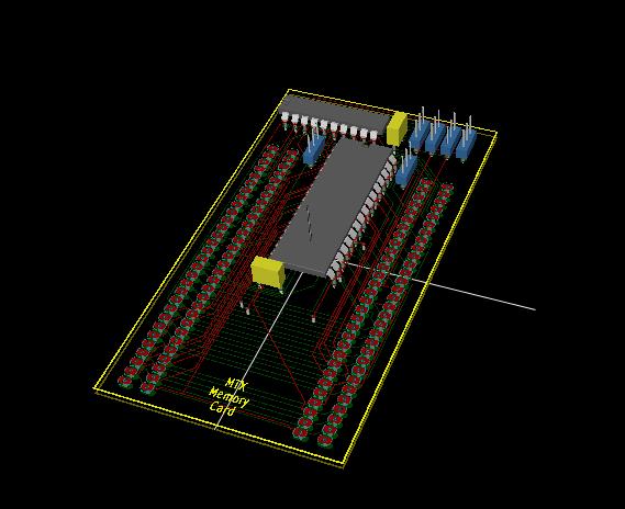
I used to KiCad to prepare this
circuit diagram.
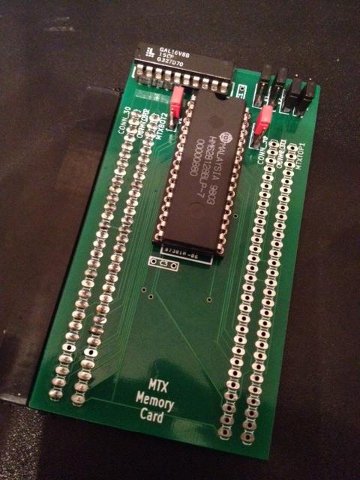
When placed and routed, and then the board manufactured and populated, you get :-


I've also added the all.tar.gz library of extra converted
parts from
http://library.oshec.org/
to my installation of KiCad.
The chips are placed as far up the card as possible, due to the
low clearance inside the MTX case.
Connectors are present on both sides, to allow insertion within the
MTX case, or outside on the left.
Note however, that Kicad doesn't seem to have footprints for connectors
allowing another adapter to be chained onto this one.
This card can use a 32KB, 64KB, 128KB, 256KB or 512KB SRAM.
There is some variability in SRAM chip pinouts.
Jumpers K5 and K6 are therefore set according to chip vendor and size :-
| Vendor | Chip | Size | Pin 1 | K5 | Pin 30 | K6 | Comments
|
|---|
| Hitachi | HM62832 | 32KB | empty | either | 5V | high | 28 pin chip placed in sockets 3 to 30
|
| Samsung | K6T0808C1D | 32KB | empty | either | 5V | high | 28 pin chip placed in sockets 3 to 30
|
| Hitachi | HM62864 | 64KB | NC | either | CS2 | high |
|
| Alliance | AS6C1008 | 128KB | NC | either | CS2 | high |
|
| Hitachi | HM628128 | 128KB | NC | either | CS2 | high |
|
| Alliance | AS6C2008 | 256KB | A17 | low | CS2 | high | lets use pin 1 as A17
|
| Alliance | AS6C4008 | 512KB | A18 | high | A17 | low | new plan, lets sacrifice CS2 on pin 30 instead
|
| Samsung | K6T4008C1B | 512KB | A18 | high | A17 | low |
|
| Hitachi | HM628512 | 512KB | A18 | high | A17 | low |
|
| Winbond | W27C512 * | 64KB | empty | either | 5V | high | 28 pin EEPROM placed in sockets 3 to 30
|
A GAL16V8 decides when the SRAM is accessed, and which part of it.
GALs support a limited amount of logic complexity.
It is not always possible to make all of the SRAM available to the MTX.
In addition to IOBYTE and address information from the MTX, this chip
is also influenced by 4 jumpers (K1 to K4).
So it is possible to have a memory card that offers different amounts of
memory, depending on the jumpers.
RAM card
MTX memory map (establishing a standard name for each 16KB RAM page) :-
| RELCPM=0 | RELCPMH=1 | Both
|
|---|
| 0x0000..0x3fff | 0x4000..0x7fff | 0x8000..0xbfff
|
|---|
| ROMs | γ | β
| | a | δ
| | c | b
| | e | d
| | g | f
| | i | h
| | k | j
| | m | l
| | o | n
| | q | p
| | s | r
| | u | t
| | w | v
| | y | x
| | A | z
| | C | B
|
|
| 0x0000..0x3fff | 0x4000..0x7fff | 0x8000..0xbfff
|
|---|
| δ | γ | β
| | a | b | c
| | d | e | f
| | g | h | i
| | j | k | l
| | m | n | o
| | p | q | r
| | s | t | u
| | v | w | x
| | y | z | A
| | B | C | D
| | E | F | G
| | H | I | J
| | K | L | M
| | N | O | P
| | Q | R | S
|
|
| 0xc000..0xffff | P3,P2,P1,P0
|
|---|
| α | 0
|
|---|
| 1
| | 2
| | 3
| | 4
| | 5
| | 6
| | 7
| | 8
| | 9
| | A
| | B
| | C
| | D
| | E
| | F
|
|
What pages do you have :-
- If you have an MTX500,
then you have pages α and β.
- If you have an MTX512 (or MTX500 with 32KB upgrade),
then you also have γ and δ.
- If you have an MTX512 S2,
then you also have a to i in RELCPMH=1 mode only.
- If removed the memory on the motherboard,
then you actually don't have any of the above after all.
- If you have a 512KB memory card,
then you have pages a to F.
- If you have a SDX card with 512KB memory installed,
then you have pages a to F.
- If you use the MTX Memory Card described on this page,
then you can add pages which you do not already have.
What can you do with the memory :-
- If you have the α, β, γ and δ pages,
then you can play all the known MTX games.
- If you have pages a to i in RELCPMH=1 mode,
and you run CP/M,
then you can configure a 512KB type 51 RAM Disc,
providing you shrink it down to 144KB using
S2R.COM.
- If you have pages a to p in RELCPMH=1 mode,
and you run CP/M,
then you can configure a 256KB type 50 RAM Disc.
- If you have pages a to F,
and you run CP/M,
then you can configure a 512KB type 51 RAM Disc.
This package includes PALASM source for various combinations of
existing memory on the motherboard, and SRAM size on the memory card.
Not all combinations are tested.
Files available cover :-
- Adding α, β, γ and δ pages
in both RELCPMH modes,
and then pages a onwards in RELCPMH=1 mode only.
This is for MTX motherboards with no memory.
- Adding γ and δ pages in both RELCPMH modes,
and then pages a onwards in RELCPMH=1 mode only.
This is for upgrading MTX500s.
- Adding pages a onwards in RELCPMH=1 mode only.
This is for upgrading MTX512s.
- Adding pages j onwards in RELCPMH=1 mode only.
This is for upgrading MTX512 S2s.
You'll observe that I haven't written any PALASM that makes
pages a onwards visible in RELCPMH=0 mode.
I'm not aware of any MTX BASIC program, or any games,
needing more than 64KB of memory to work.
Pages a onwards are visible in RELCPMH=1 mode not because any CP/M
program is known to directly use them, but rather because this memory
can be configured as RAM Disc.
Attempting to make pages a onwards in RELCPMH=0 mode would
require many more terms in the PALASM expressions, and GAL16V8
expressions can only have 8 terms OR'ed together.
This limit is much better than the 4 term limit that PAL14L4s had,
but even this enlarged limit already prevents us making 100%
effective use of the space in larger SRAMs.
Trying to support pages a onwards in RELCPMH=0 would make this
much worse.
So, I'll need someone to provide a good justification before
attempting to write PALASM for this.
ROM card
It should also be possible to make this memory card work with EEPROM,
in a somewhat limited fashion, although not as a conventional ROM card.
A 64KB W27C512 EEPROM is almost pin compatible with a 32KB HM62832 SRAM.
Here are the differences :-
| Socket pin | Chip pin | W27C512 | HM62832
|
|---|
| 3 | 1 | A15 | A14
|
| 29 | 27 | A14 | /WE
|
This means that 2 16KB address ranges (0x0000-0x3fff and 0x8000-0xbfff)
of the EEPROM can be made visible to the system.
But note that A13 and ROM Page bits R2-R0 are not passed in to the GAL,
which prevents us from putting the EEPROM content in the usual ROM slots.
If A13 and R2-R0 were "yellow wired" to K3 and K2-K0, this could be fixed.
Cost
If you shop around :-
| Item | Cost
|
|---|
| PCB | £3
|
| SRAM chip | £3
|
| GAL16V8 | £1
|
| MTX edge-connector | £2
|
| Passives, headers, sockets, etc... | £1
|
| Total | £10
|
Download
Full package downloadable from
here.
This page maintained by Andy Key
andy.z.key@googlemail.com

